Get Started with IP Core Generation for Intel SoC Devices
This example shows how to use the Simulink Toolstrip and Simulink Interface along with the hardware-software co-design workflow to blink LEDs at various frequencies on the Arrow® SoCKit® evaluation kit.
Introduction
This example is a step-by-step guide that helps you use the HDL Coder™ software to generate a custom HDL IP core which blinks LEDs on the Arrow SoCKit evaluation kit, and shows how to use Embedded Coder® to generate C code that runs on the ARM® processor to control the LED blink frequency.
You can use MATLAB® and Simulink® to design, simulate, and verify your application, perform what-if scenarios with algorithms, and optimize parameters. You can then prepare your design for hardware and software implementation on the Altera Cyclone V SoC by deciding which system elements will be performed by the programmable logic, and which system elements will run on the ARM Cortex-A9.
Using the guided workflow shown in this example, you automatically generate HDL code for the programmable logic using HDL Coder, generate C code for the ARM using Embedded Coder, and implement the design on the Intel SoC devices.
In this workflow, you perform the following steps:
Set up your Intel SoC hardware and tools.
Partition your design for hardware and software implementation.
Generate an HDL IP core using HDL Workflow Advisor.
Integrate the IP core into a Intel Qsys project and program the Intel SoC hardware.
Generate a software interface model.
Generate C code from the software interface model and run it on the ARM Cortex-A9 processor.
Tune parameters and capture results from the Intel SoC hardware using External Mode.
For more information, refer to other more advanced examples, and the HDL Coder and Embedded Coder documentation.
Requirements
Intel Quartus Prime, with supported version listed in the HDL Language Support and Supported Third-Party Tools and Hardware.
Intel SoC Embedded Design Suite
Arrow SoCKit Cyclone V SoC evaluation kit
HDL Coder Support Package for Intel FPGA and SoC Devices
Embedded Coder Support Package for Intel SoC Devices
Set Up Intel SoC Hardware and Tools
1. Set up the Arrow SoCKit evaluation kit as shown in the figure below. To learn more about the Arrow SoCKit hardware setup, refer to the board documentation.

2. Set up SW4 switch (JTAG chain select) as shown in the figure below. Position 1 : OFF; Position 2 : ON. This configuration includes HPS in JTAG chain, and bypasses HSMC.

3. Set up JP2 as shown in the figure below to adjust the I/O Standard of the FPGA/HSMC pins. Short Pin 5 and 6 to set the I/O voltage to 2.5V.

4. Set up J17 - J19 as shown in the figure above to boot HPS from SD card. J17: Short Pin 1 and 2; J18: Short Pin 1 and 2; J19: Short Pin 2 and 3.
5. Set up J15 - J16 as shown in the figure above for HPS clock setting. J15: Short Pin 2 and 3; J16: Short Pin 2 and 3.
6. Set up SW6 on the back side of the board as shown in the figure below. This switch set the FPGA configuration mode. Set all 6 positions to ON.

7. Connect your computer to the USB UART connector using a Micro-USB cable. Make sure your USB device drivers, such as for the FTDI USB to UART, are installed correctly. If not, search for the drivers online and install them.
8. Connect your computer and the Arrow SoCKit board using an Ethernet cable.
9. Install the HDL Coder Support Package for Intel FPGA and SoC Devices and Embedded Coder Support Package for Intel SoC Devices if you haven't already. To start the installer, go to the MATLAB toolstrip and click Add-Ons > Get Hardware Support Packages.
10. Make sure you are using the SD card image provided by the Embedded Coder Support Package for Intel SoC Devices. If you need to update your SD card image, refer to the Add Support for Intel SoC Platform (Embedded Coder) of this document.
11. Set up the Arrow SoCKit hardware connection by entering the following command in the MATLAB command window:
h = alterasoc
The alterasoc function logs in to the hardware via COM port and runs the ifconfig command to obtain the IP address of the board. This function also tests the Ethernet connection.
12. You can optionally test the serial connection using the following configuration using a program such as PuTTY™. Baud rate: 115200; Data bits: 8; Stop bits: 1; Parity: None; Flow control: None. You should be able to observe Linux booting log on the serial console when you power cycle the Arrow SoCKit board. You must close this serial connection before using the alterasoc function again.
13. Set up the Intel Quartus Prime synthesis tool path using the hdlsetuptoolpath function.
hdlsetuptoolpath('ToolName','Altera Quartus II','ToolPath',quartusToolPath);
Use your own Intel Quartus Prime installation path when you run this command. For more information, see hdlsetuptoolpath.
Partition Design for Hardware and Software Implementation
The first step of the Intel SoC hardware-software co-design workflow is to decide which parts of your design to implement on the programmable logic, and which parts to run on the ARM processor.
Group all the blocks you want to implement on programmable logic into an atomic subsystem. This atomic subsystem is the boundary of your hardware-software partition. All the blocks inside this subsystem will be implemented on programmable logic, and all the blocks outside this subsystem will run on the ARM processor.
In this example, the subsystem led_counter is the hardware subsystem. It models a counter that blinks the LEDs on an FPGA board. Two input ports, Blink_frequency and Blink_direction, are control ports that determine the LED blink frequency and direction. All the blocks outside of the subsystem led_counter are for software implementation.
In Simulink, you can use the Slider Gain or Manual Switch block to adjust the input values of the hardware subsystem. In the embedded software, this means the ARM processor controls the generated IP core by writing to the AXI interface accessible registers. The output port of the hardware subsystem, LED, connects to the LED hardware. The output port, Read_Back, can be used to read data back to the processor.
open_system('hdlcoder_led_blinking_4bit');
Generate HDL IP Core
Since R2023b
Next, configure your model for IP core generation, configure your design and target interface, and generate the IP core. This example uses the HDL Code tab in the Simulink Toolstrip to generate an IP core. The generated IP core is designed to be connected to an embedded processor on an FPGA device. HDL Coder generates HDL code from the Simulink blocks, and also generates HDL code for the AXI interface logic that connects the IP core to the embedded processor. HDL Coder packages the generated files into a folder you specify. You can then integrate the generated IP core with a larger FPGA embedded design in the Intel Qsys environment.
For an overview of how to generate an IP core for a specific hardware platform, see Targeting FPGA & SoC Hardware Overview. For more information on different ways to generate an IP core using HDL Coder, see Comparison of IP Core Generation Techniques.
Prepare Model for IP Core Generation
To generate an IP core from the hdlcoder_led_blinking_4bit/led_counter subsystem, prepare your model by using the configuration parameters, configure your design by using the IP Core editor, and generate the IP core by using the HDL Code tab of the Simulink Toolstrip.
In the Apps tab, click HDL Coder. In the HDL Code tab, in the Output section, set the drop-down button to IP Core.
Select the
led_countersubsystem which is the device under test (DUT) for this example. Make sure that Code for is set to this subsystem. To remember the selection, you can click the pin button .
. 
Click Setting to open the HDL Code Generation > Target pane of the Configuration Parameters dialog box.
Set the Target Platform parameter to
Arrow SoCKit development board. If this option does not appear, select Get more to open the Support Package Installer. In the Support Package Installer, select Intel FPGA and SoC Devices and follow the instructions to complete the installation. Ensure the Synthesis Tool is set toAltera QUARTUS II.Ensure that the Reference Design parameter is set to
Default system.Set the Target Frequency to
50MHz.Click OK to save your updated settings.
Configure Design and Target Interface
Configure your design to map to the target hardware by mapping the DUT ports to IP core target hardware and setting DUT-level IP core options. In this example, the input ports Blink_frequency and Blink_direction are mapped to the AXI4 interface, so HDL Coder generates AXI interface accessible registers for them. The LED output port is mapped to an external interface, LEDs General Purpose [0:3], which connects to the LED hardware on the Intel SoC board.
In Simulink, in the HDL Code tab, click Target Interface to open the IP Core editor.
Select the Interface Mapping tab to map each DUT port to one of the IP core target interfaces. If no mapping table appears, click the Reload IP core settings
 button to compile the model and repopulate the DUT ports and their data types.
For the DUT ports Blink_frequency, Blink_direction, and Read_back, set the cells in the Interface column to
AXI4.For the LED output port, set the cell in the Interface column to
LEDs General Purpose [0:3].
Validate your settings by clicking the Validate IP core settings
 button.
In the IP Core editor, you can optionally adjust the DUT-level IP core settings for your target hardware by:
Using the General tab to configure top-level settings, such as the name of the IP core and whether to generate an IP core report.
Using the Clock Settings tab to configure clock-related settings.
Using the Interface Settings tab to configure interface-related settings, such as the register interface and FPGA data capture properties.
Generate IP Core
Next generate the IP core. In the Simulink Toolstrip, in the HDL Code tab, click Generate IP Core. After you generate the custom IP core, the IP core files are in the ipcore folder in your current directory. To specify a top-level project folder for the ipcore folder to be stored along with all other generated files, in the Configuration Parameters dialog box, use the Project Folder parameter in the HDL Code Generation > Target tab. If the Project Folder parameter is empty, HDL Coder saves the generated files in the current directory.
Generating an IP core also generates the code generation report. In the Code Generation Report window, in the left pane, click the IP Core Generation Report. The report describes the behavior and contents of the generated custom IP core.

Integrate IP Core with Intel Qsys
Since R2023b
Next, insert your generated IP core into an embedded system reference design by creating a project, generating an FPGA bitstream, and downloading the bitstream to the Intel SoC hardware.
The reference design is a predefined Intel Qsys project that contains the elements the Intel software needs to deploy your design to the Intel SoC device, except for the custom IP core and embedded software that you generate. This example uses the HDL Code tab in the Simulink Toolstrip to deploy and verify an IP core. For more information on how to deploy and verify an IP Core using the HDL workflow advisor, see Comparison of IP Core Deployment and Verification Techniques.
Create IP Core Project
Integrate your generated IP core into the Intel platform by creating a Qsys project that organizes and maintains the files associated with the IP core. To create a Qsys project in the Simulink Toolstrip, in the HDL Code tab, select Build Bitstream > Create IP Core Project. HDL Coder generates an IP integrator embedded design and displays the link to it in the Diagnostic Viewer.

Configure Deployment Settings
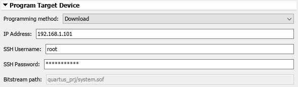
Next, configure the build bitstream settings. In the Simulink Toolstrip, in the HDL Code tab, select Build Bitstream > Deployment Settings. In the Deployment Settings window, under the Build Bitstream section, select Run build process externally to run the Intel synthesis tool in a separate window than the current MATLAB session.

In the Program Target Device section:
Set Programming method to
Downloadto download the bitstream to your target Intel SoC board SD card and load your design when the board power cycles.Set IP Address to your target board IP address.
Set SSH username and SSH Password to your target board settings.
Generate Bitstream and Program Target Device
To generate the bitstream file, in the Simulink Toolstrip, in the HDL Code tab, click Build Bitstream and wait until the synthesis tool runs in the external window.
To download the bitstream, in the Simulink Toolstrip, in the HDL Code tab**,** select Build Bitstream > Program Target Device.
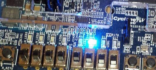
After you program the FPGA hardware, the LED starts blinking on your Intel SoC board.
Prototype and Verify IP Core on Hardware
Verify your generated IP core on the hardware by using MATLAB to generate a host interface script. This script contains MATLAB commands that connect your hardware and interact with your IP core. To generate a host interface script file, in the Simulink Toolstrip, in the HDL Code tab, select Host Interface Script > Host Interface Script.


HDL Coder generates two MATLAB files in your current folder that enable you to prototype your generated IP core directly from MATLAB.
![]()
Open the generated interface script file by clicking the link in the Simulink Diagnostic Viewer. This file creates a connection to your FPGA hardware that reads and writes data and configures the fpga hardware object with the same ports and interfaces that you mapped in the Target Interface table. You can reuse this function in your own scripts to recreate this configuration. For example, uncomment the lines with the writePort function in the gs_hdlcoder_led_blinking_4bit_interface.m function and modify it to change the LED blink frequency. Run the modified script and observe that the LED blink frequency changes on the hardware. In addition, uncomment lines with the readPort function in the gs_hdlcoder_led_blinking_interface.m function and observe the change in values by reading back the data values.

Deploy to Processor Using Software Interface Model
To target a portion of your design for the ARM processor, generate a software interface model. The software interface model contains the part of your design that runs in software. It includes the blocks outside of the HDL subsystem, and replaces the HDL subsystem with AXI driver blocks. If you have an Embedded Coder license, you can automatically generate embedded code from the software interface model, build it, and run the executable on Linux on the ARM processor. The generated embedded software generates AXI driver code from the AXI driver blocks and uses the code to control the HDL IP core. You can generate the software interface model at any stage of the IP core generation and IP core integration process.
To generate the software interface model, in the Simulink Toolstrip, in the HDL Code tab, select Build Bitstream > Software Interface Model. The Simulink Diagnostic Viewer displays a link to the generated software interface model.

The generated software interface model replaces the led_counter subsystem with the AXI driver blocks that generate the interface logic between the ARM processor and FPGA.

Run Software Interface Model on Intel SoC Hardware
Next, configure the generated software interface model, generate the embedded C code, and run your model on the ARM processor in the Intel SoC hardware in external mode.
When you prototype and develop an algorithm, it is useful to monitor and tune the algorithm while it runs on hardware. You can use external mode to deploy your algorithm to the ARM processor in the Intel SoC hardware, and then link the algorithm with the Simulink model on the host computer through an Ethernet connection.
The Simulink model tunes and monitors the algorithm running on the hardware. Because the ARM processor is connected to the HDL IP core through the AXI interface, you can use external mode to tune parameters, and capture data from the FPGA.

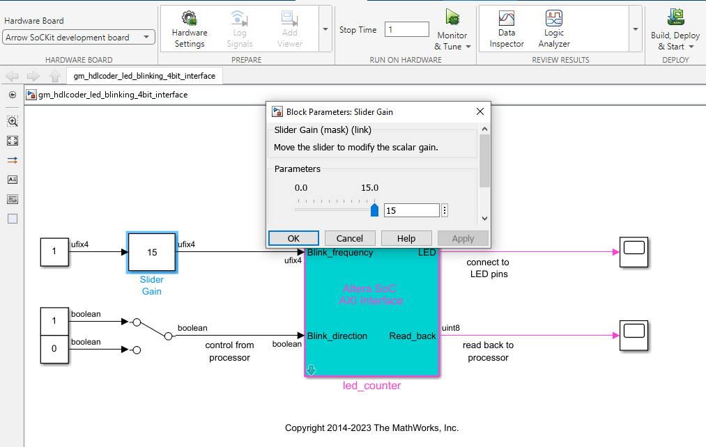
In the generated model, in the Hardware tab, in the Prepare section, click Hardware settings to open the Configuration Parameters dialog box.
In the Run On Hardware section, set Stop time to
inf.Click Monitor & Tune to run your model on the ARM processor in the Intel SoC hardware in external mode. Embedded Coder builds the model, downloads the ARM executable to the Intel SoC hardware, executes it, and connects the model to the executable.
Double-click the Slider Gain block. Change the slider and observe the change in frequency of the LED array blinking on the Intel SoC hardware. Double-click the Manual Switch block to switch the direction of the blinking LEDs.
Double-click the Scope block connected to the Read_back output port. The Scope block captures the output data of the FPGA IP core.
When you are done changing model parameters, click the Stop button in the toolstrip, then close the system command window.