PCB アンテナの設計および製造
Antenna Toolbox™ を使用して、携帯電話、RFID、IoT アプリケーションなどの実用的な設計向けにカスタム プリント基板 (PCB) アンテナを設計します。用途に適した RF コネクタを指定し、PCB 製造サービスをカスタマイズすることで、シミュレーション済み PCB アンテナのプロトタイプ作成と実装を行います。
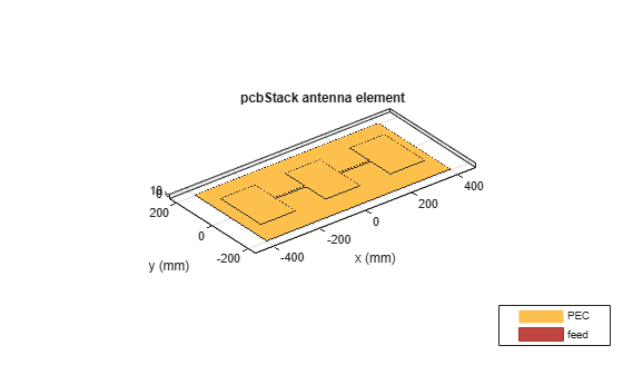
幾何学的形状と数学的演算を組み合わせて、アンテナ仕様に適合する独自のアンテナ ジオメトリを作成します。たとえば、pcbStack オブジェクトを使用して、形状オブジェクトとその関数で、単層または多層の PCB ベースのアンテナ設計を作成できます。
このカテゴリの PCB 製造オブジェクトと PCB 製造関数を使用して、ガーバー ファイルによる (PCB) 設計の読み書きを行います。
単一給電またはマルチ給電の PCB アンテナを対話的に設計、解析、エクスポートするには、PCB アンテナ デザイナー アプリを使用します。
アプリ
| PCB アンテナ デザイナー | Design, analyze, optimize, and export single or multifeed PCB antennas (R2021b 以降) |
オブジェクト
関数
トピック
- Board Thickness versus Dielectric Thickness in PCB
Define board and dielectric thickness of a PCB antenna for various scenarios like single and multi-layer dielectric, and imported designs from Gerber files. (R2022b 以降)
注目の例

Design Wideband Cellular Base Station Antenna with Parasitic Elements
Design a custom antenna with parasitic elements to enhance its directivity and bandwidth for cellular base station applications.
Modeling and Analysis of 5G NR FR1 Ultra-Wideband Antenna
Model a 5G NR FR1 Ultra-wideband antenna having a coplanar structure with no ground plane and an arbitrary finite gap feed.

Model Coaxial Gap Feed for Probe-Fed Patch Antenna
Comparison of a standard delta-gap probe feed model and a finite-gap coaxial feed model for a patch antenna.

PCB アンテナ デザイナーを使用した設計と解析
1 行 2 列の H ノッチ直線アンテナ アレイを設計、検証、解析、およびエクスポートする。

Dual-Fed Square Microstrip Patch Antenna for BLE Applications
Design and analyze the dual-fed square microstrip patch antenna for Bluetooth Low Energy applications.

Corporate Feed Divider Network for a Linear Patch Antenna array
Integrate a corporate power divider with a microstrip patch antenna array. The corporate power divider is available as a catalog element in RF PCB Toolbox. The patch antenna array is built using the patchMicrostripInsetfed catalog element and pcbStack from Antenna Toolbox.

Design, Analyze, and Prototype 2-by-2 Patch Antenna Array
Design and analysis of a 2‑by‑2 microstrip patch antenna array on an FR4 substrate operating at 2.4 GHz, including full simulation and generation of PCB Gerber files for fabrication.
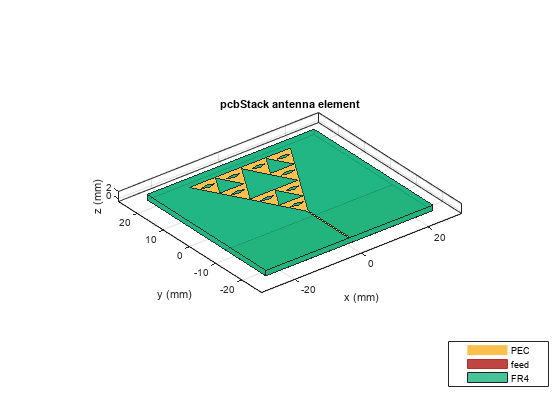
Modified Sierpinski Monopole Fractal Antenna for Dual-Band Application
Model and analyze a compact second‑order modified Sierpinski fractal monopole antenna on an FR4 substrate for dual‑band S‑ and C‑band operation.

Create Antenna Model from Gerber Files
Create an antenna model from Gerber files and subsequently analyze the antenna. The Gerber file format is used in printed circuit board (PCB) manufacturing and is defined in the RS-274X standard which is the newer extended Gerber format. The Antenna Toolbox™ supports the newer RS-274X format both to generate Gerber files from an antenna model as well as to create an antenna model from a set of Gerber files.

Design, Analysis, and Prototyping of Microstrip-Fed Wide-Slot Antenna
Model a microstrip-fed printed wide slot antenna with an FR4 substrate, analyze it, and finally generate Gerber files to enable its prototyping. The design is intended for operation in the L-band and has a bandwidth of about 17% over the band 1.6 - 1.8 GHz.
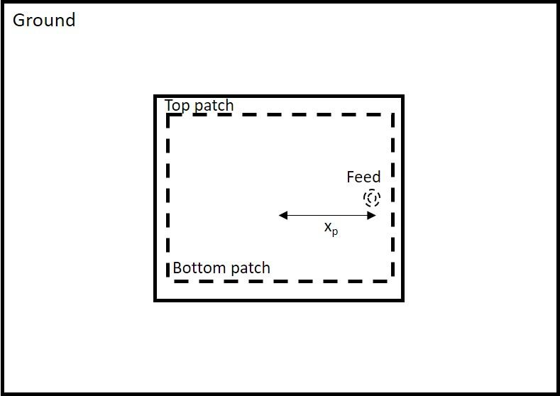
Modeling and Analysis of Probe-Fed Stacked Patch Antenna
The steps to model and analyze a probe-fed stacked patch antenna. The standard rectangular microstrip patch antenna has a narrow impedance bandwidth typically less than 5%. The stacked patch configuration is one of the ways of increasing the impedance bandwidth of these antennas to be greater than 25% [1]. There are different ways of designing stacked patches, primarily differing in the way their feed is designed [2]. The two types of feeding mechanisms are probe-feed and aperture coupled. These two mechanisms have a role in the impedance bandwidth behavior as well as the radiation characteristics of the antenna.

Model and Analyze Dual Polarized Patch Microstrip Antenna
Design and measure a wideband dual polarized microstrip antenna that finds its use at the base station of a cellular system. In order to achieve the wideband characteristics, this design considers a slot coupled patch antenna structure.

Modeling and Analysis of Single Layer Multi-Band U-Slot Patch Antenna
The standard rectangular microstrip patch is a narrowband antenna and provides 6-8 dBi Gain with linear polarization. This example is based on the work done in [1],[2], and models a broadband patch antenna using a slot in the radiator and develops a dual-band and a tri-band variation from it. In the process, the single wide response is split into multiple narrow band regions catering to specific bands in the WiMAX standard. These patch antennas are probe-fed.
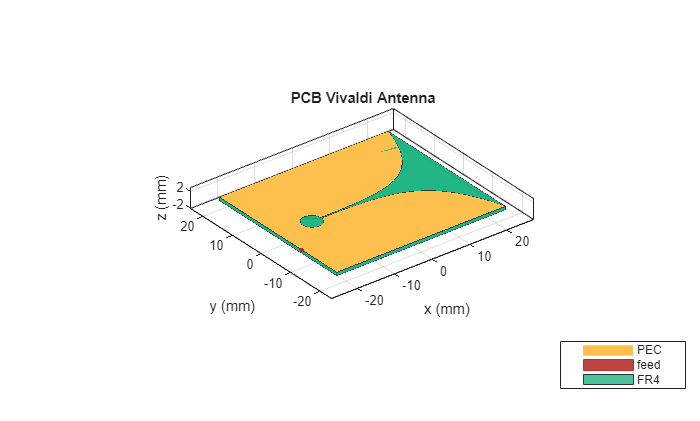
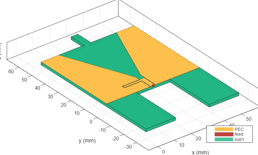
Design Internally Matched Ultra-Wideband Vivaldi Antenna
Model and analyze a vivaldi antenna with an internal matching circuit. The vivaldi is also known as an exponentially tapered slot antenna. The antenna possesses wideband characteristics, low cross polarization and a highly directive pattern. The design is implemented on a single layer dielectric substrate with 2 metal layers; one for a flared slot line, and the feed line with the matching circuit on the other layer. The substrate is chosen as a low cost FR4 material of thickness 0.8 mm. The design is intended for operation over the frequency band 3.1 - 10.6 GHz [1].

Design and Analysis of Compact Ultra-Wideband MIMO Antenna Array
Design and analysis of a compact ultra‑wideband MIMO antenna array operating from 3.1 to 10.6 GHz to address multipath fading and enhance channel capacity in UWB systems.
PCB スタックを使用したマイクロストリップ パッチ アンテナの設計バリエーション
pcbstack を使用して、基本パッチ アンテナ、寄生パッチ アンテナ、直接結合パッチ アンテナ、CP パッチ アンテナを設計します。