PCBWriter
Create PCB board definitions from 2-D antenna designs
Description
Use the PCBWriter object to create a printed circuit board
(PCB) design files based on multilayer 2-D antenna design. A set of manufacturing files
known as Gerber files describes a PCB antennas. A Gerber file uses an ASCII vector
format for 2-D binary images.
Creation
Syntax
Description
b = PCBWriter(pcbstackobject)PCBWriter object that generates Gerber-format
PCB design files based on a 2-D antenna design geometry using PCB
stack.
b = PCBWriter(pcbstackobject,rfconnector)rfconnector
type.
b = PCBWriter(pcbstackobject,writer)writer.
b = PCBWriter(pcbstackobject,rfconnector,writer)
Input Arguments
Single feed PCB antenna, specified as a pcbStack object.
Example: p1 = pcbStack;
a = PCBWriter(p1); creates a
PCBWriter object from PCB stack.
Service to view PCB design, specified as a PCBServices object.
Example: s = PCBServices.MayhewWriter;
a = PCBWriter(p1,s); uses Mayhew Labs PCB service to
view the PCB design.
RF connector type for PCB antenna feedpoint, specified as a PCBConnectors object.
Example: c = PCBConnectors.SMA_Cinch;
a = PCBWriter(p1,c); uses SMA_Cinch RF connector at
feedpoint.
Output Arguments
PCB Board definition of 2.5D antenna design, returned as an object.
Properties
This property is read-only.
PCB Antenna geometry information, represented as a structure. The geometry information includes:
Layers— Vector of structures describing all metal layers.FeedLocations— Cell vector defining antenna feed points.ViaLocations— Cell vector specifying electrical connections (shorts) between pairs of metal layers in the antenna at specified locations.ViaDiameter— Diameter of the electrical shorts.DefaultConnector— Default RF connector to add to the PCB, when no connector is specified.DesignInfo— Structure containing title, comment, and attribute text for the PCB design.Source— Source of the PCB design.
Data Types: struct
PCB manufacturing service to view PCB design, specified as a PCBServices object.
Example: a = PCBWriter; a.Writer =
PCBService.MayhewWriter; uses Mayhew Labs PCB service to view
the PCB design.
RF connector type for PCB antenna feedpoint, specified as a PCBConnectors object.
Example: a = PCBWriter(pcbStack); a.Connector =
PCBConnectors.SMA_Cinch; uses SMA_Cinch RF connector at the
feedpoint.
Use default connector, specified as 0 or
1.
Example: a.UseDefaultConnector = 1, where
a is a PCBWriter
object.
Data Types: logical
Line widths drawn around components on silk screens, specified as a positive scalar in mils.
Example: a.ComponentBoundaryLineWidth = 10, where
a is a PCBWriter
object.
Data Types: double
Font size to label components on silk screen, specified as a positive scalar in points.
Example: a.ComponentNameFontSize = 12, where
a is a PCBWriter
object.
Data Types: double
Design information text font size added outside board profile, specified as a positive scalar.
Example: a.DesignInfoFontSize = 12, where
a is a PCBWriter
object.
Data Types: double
Font used for component name and design info, specified as a character vector.
Example: a.Font = 'TimesNewRoman', where
a is a PCBWriter
object.
Data Types: char | string
Copper free margin around board, specified as a positive scalar in meters.
Example: a.PCBMargin = 0.7e-3, where
a is a PCBWriter
object.
Data Types: double
Add solder mask to top and bottom of PCB, specified as
'both', 'top',
'bottom' or 'none'.
Example: a.SolderMask = 'top', where
a is a PCBWriter
object.
Data Types: char | string
Generate solder paste files as a part of PCB stack, specified as
1 or 0.
Example: a.SolderPaste = 0, where a
is a PCBWriter object.
Data Types: logical
Enable or disable watermark signature, specified as a logical value. By
default, the signature is enabled. Specify value as 0 to
disable the signature.
Example: a.EnableSignature=0, where a
is a PCBWriter object.
Data Types: logical
Enable or disable connector labels, specified as a logical value. By
default, the connector label is enabled. Specify value as
0 to disable the connector label.
Example: a.EnableConnectorLabel=0, where
a is a PCBWriter
object.
Data Types: logical
Object Functions
gerberWrite | Generate Gerber files |
openFolder | Open folder containing generated Gerber files in files browser |
sendTo | Export generated Gerber Files to service provider |
Examples
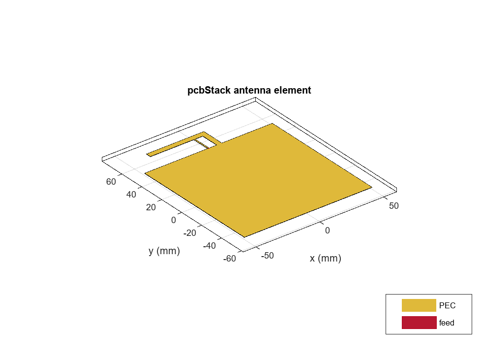
Create a coplanar inverted-F antenna.
fco = invertedFcoplanar(Height=14e-3,GroundPlaneLength=100e-3,...
    GroundPlaneWidth=100e-3);
Create a pcbStack object.
p = pcbStack(fco);
figure
show(p)
title("Inverted-F PCB Antenna")
Generate a Gerber format design file using PCB Writer.
PW = PCBWriter(p)
PW =
  PCBWriter with properties:

                        Design: [1×1 struct]
                        Writer: [1×1 Gerber.Writer]
                     Connector: []
           UseDefaultConnector: 1
    ComponentBoundaryLineWidth: 8
         ComponentNameFontSize: []
            DesignInfoFontSize: []
                          Font: 'Arial'
                     PCBMargin: 5.0000e-04
                    Soldermask: 'both'
                   Solderpaste: 1
               EnableSignature: 1
          EnableConnectorLabel: 1

   See info for details
Create a coplanar inverted-F antenna.
fco = invertedFcoplanar(Height=14e-3,GroundPlaneLength=100e-3,...
    GroundPlaneWidth=100e-3);
Create a pcbStack object.
p = pcbStack(fco);
figure
show(p)
title("Inverted-F PCB Antenna")
Create an SMA_Cinch connector using the PCBConnectors object.
c = PCBConnectors.SMA_Cinch
c =
  SMA_Cinch with properties:

                    Type: 'SMA'
                     Mfg: 'Cinch'
                    Part: '142-0711-202'
              Annotation: 'SMA'
               Impedance: 50
               Datasheet: 'https://belfuse.com/resources/Johnson/drawings/dr-142-0711-202.pdf'
                Purchase: 'https://www.digikey.com/product-detail/en/cinch-connectivity-solutions-johnson/142-0711-202/J10154TR-ND/3587681'
               TotalSize: [0.0071 0.0071]
           GroundPadSize: [0.0024 0.0024]
       SignalPadDiameter: 0.0017
         PinHoleDiameter: 0.0013
           IsolationRing: 0.0041
    VerticalGroundStrips: 1

   Cinch 142-0711-202 (Example Purchase)
Create a PCB design file for the antenna with the connector.
PW = PCBWriter(p,c)
PW =
  PCBWriter with properties:

                        Design: [1×1 struct]
                        Writer: [1×1 Gerber.Writer]
                     Connector: [1×1 PCBConnectors.SMA_Cinch]
           UseDefaultConnector: 0
    ComponentBoundaryLineWidth: 8
         ComponentNameFontSize: []
            DesignInfoFontSize: []
                          Font: 'Arial'
                     PCBMargin: 5.0000e-04
                    Soldermask: 'both'
                   Solderpaste: 1
               EnableSignature: 1
          EnableConnectorLabel: 1

   See info for details
Create a coplanar inverted-F antenna.
fco = invertedFcoplanar(Height=14e-3,GroundPlaneLength=100e-3,...
    GroundPlaneWidth=100e-3);
Create a pcbStack object.
p = pcbStack(fco);
figure
show(p)
title("Inverted-F PCB Antenna")
Use an Advanced Circuits Writer as a PCB manufacturing service.
s = PCBServices.AdvancedCircuitsWriter
s =
  AdvancedCircuitsWriter with properties:

               BoardProfileFile: 'legend'
          BoardProfileLineWidth: 1
                 CoordPrecision: [2 6]
                     CoordUnits: 'in'
              CreateArchiveFile: 1
                 DefaultViaDiam: 3.0000e-04
             DrawArcsUsingLines: 0
                 ExtensionLevel: 1
                       Filename: 'untitled'
                          Files: {}
         IncludeRootFolderInZip: 0
                   PostWriteFcn: @(obj)sendTo(obj)
    SameExtensionForGerberFiles: 0
                    UseExcellon: 1
Create an antenna PCB design file using the above service.
PW = PCBWriter(p,s)
PW =
  PCBWriter with properties:

                        Design: [1×1 struct]
                        Writer: [1×1 PCBServices.AdvancedCircuitsWriter]
                     Connector: []
           UseDefaultConnector: 1
    ComponentBoundaryLineWidth: 8
         ComponentNameFontSize: []
            DesignInfoFontSize: []
                          Font: 'Arial'
                     PCBMargin: 5.0000e-04
                    Soldermask: 'both'
                   Solderpaste: 1
               EnableSignature: 1
          EnableConnectorLabel: 1

   See info for details
Create a coplanar inverted F antenna.
fco = invertedFcoplanar(Height=14e-3,GroundPlaneLength=100e-3,...
                  GroundPlaneWidth=100e-3);
Use this antenna to create a pcbStack object.
p = pcbStack(fco)
p =
  pcbStack with properties:

              Name: 'Coplanar Inverted-F'
          Revision: 'v1.0'
        BoardShape: [1×1 antenna.Rectangle]
    BoardThickness: 0.0013
            Layers: {[1×1 antenna.Polygon]}
     FeedLocations: [0 0.0500 1]
      FeedDiameter: 5.0000e-04
      ViaLocations: []
       ViaDiameter: []
      FeedViaModel: 'strip'
       FeedVoltage: 1
         FeedPhase: 0
         Conductor: [1×1 metal]
              Tilt: 0
          TiltAxis: [1 0 0]
              Load: [1×1 lumpedElement]
figure
show(p)

Use an SMA_Cinch as an RF connector and Mayhew Writer as a 3-D viewer.
c = PCBConnectors.SMA_Cinch
c =
  SMA_Cinch with properties:

                    Type: 'SMA'
                     Mfg: 'Cinch'
                    Part: '142-0711-202'
              Annotation: 'SMA'
               Impedance: 50
               Datasheet: 'https://belfuse.com/resources/Johnson/drawings/dr-142-0711-202.pdf'
                Purchase: 'https://www.digikey.com/product-detail/en/cinch-connectivity-solutions-johnson/142-0711-202/J10154TR-ND/3587681'
               TotalSize: [0.0071 0.0071]
           GroundPadSize: [0.0024 0.0024]
       SignalPadDiameter: 0.0017
         PinHoleDiameter: 0.0013
           IsolationRing: 0.0041
    VerticalGroundStrips: 1

   Cinch 142-0711-202 (Example Purchase)
s = PCBServices.MayhewWriter
s =
  MayhewWriter with properties:

               BoardProfileFile: 'legend'
          BoardProfileLineWidth: 1
                 CoordPrecision: [2 6]
                     CoordUnits: 'in'
              CreateArchiveFile: 0
                 DefaultViaDiam: 3.0000e-04
             DrawArcsUsingLines: 1
                 ExtensionLevel: 1
                       Filename: 'untitled'
                          Files: {}
         IncludeRootFolderInZip: 0
                   PostWriteFcn: @(obj)sendTo(obj)
    SameExtensionForGerberFiles: 0
                    UseExcellon: 1
Create an antenna design file using PCBWriter.
PW = PCBWriter(p,s,c)
PW =
  PCBWriter with properties:

                        Design: [1×1 struct]
                        Writer: [1×1 PCBServices.MayhewWriter]
                     Connector: [1×1 PCBConnectors.SMA_Cinch]
           UseDefaultConnector: 0
    ComponentBoundaryLineWidth: 8
         ComponentNameFontSize: []
            DesignInfoFontSize: []
                          Font: 'Arial'
                     PCBMargin: 5.0000e-04
                    Soldermask: 'both'
                   Solderpaste: 1

   See info for details
Use the gerberWrite function to generate gerber files from the antenna design files. Send the generated files to the Mayhew writer manufacturing service.
gerberWrite(PW)
The default folder containing the gerber files is named "untitled" and is located in your MATLAB folder. Running this example automatically opens up the Mayhew Labs PCB manufacturing service in your internet browser.

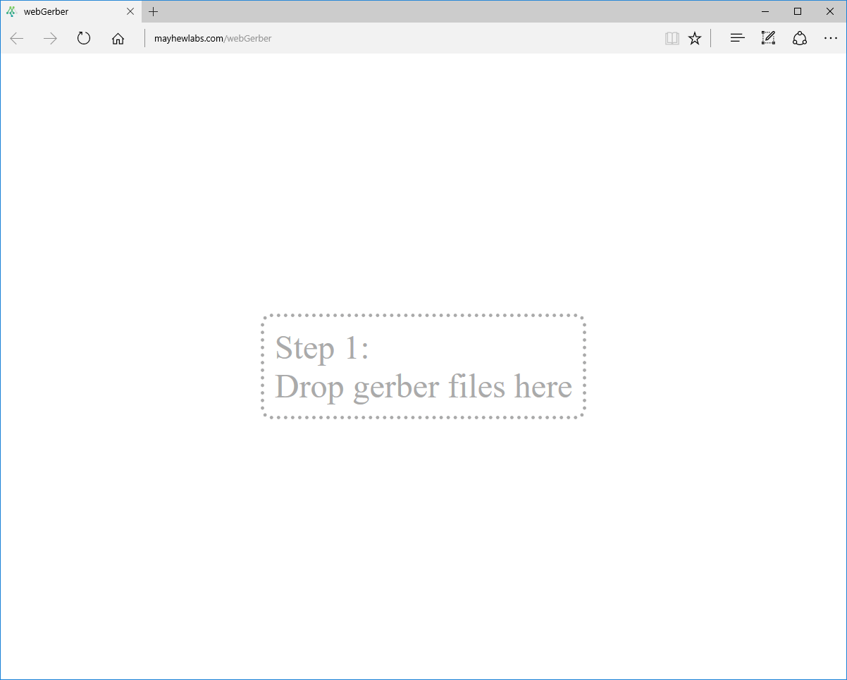
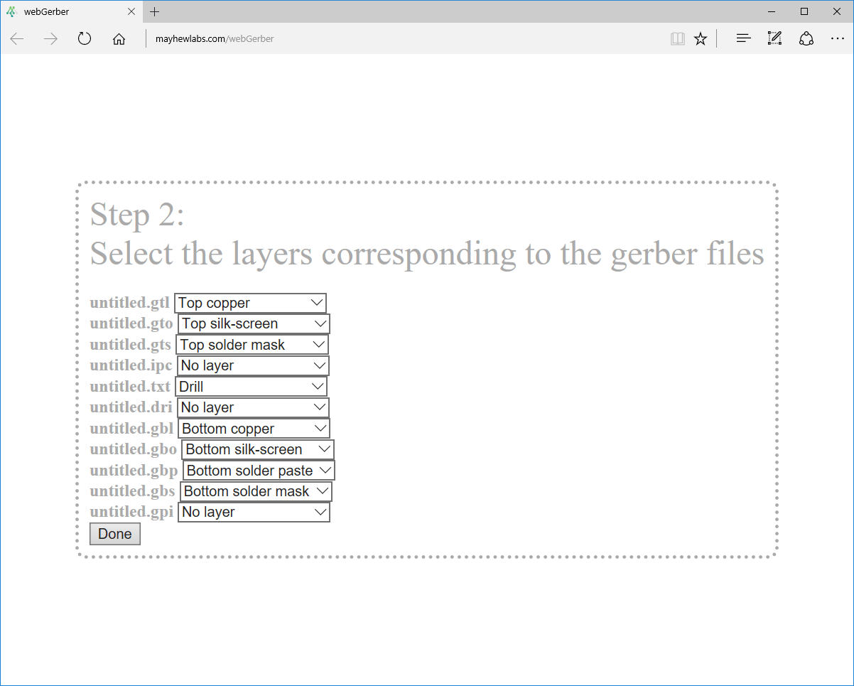
Drag and drop all your files from the "untitled" folder.

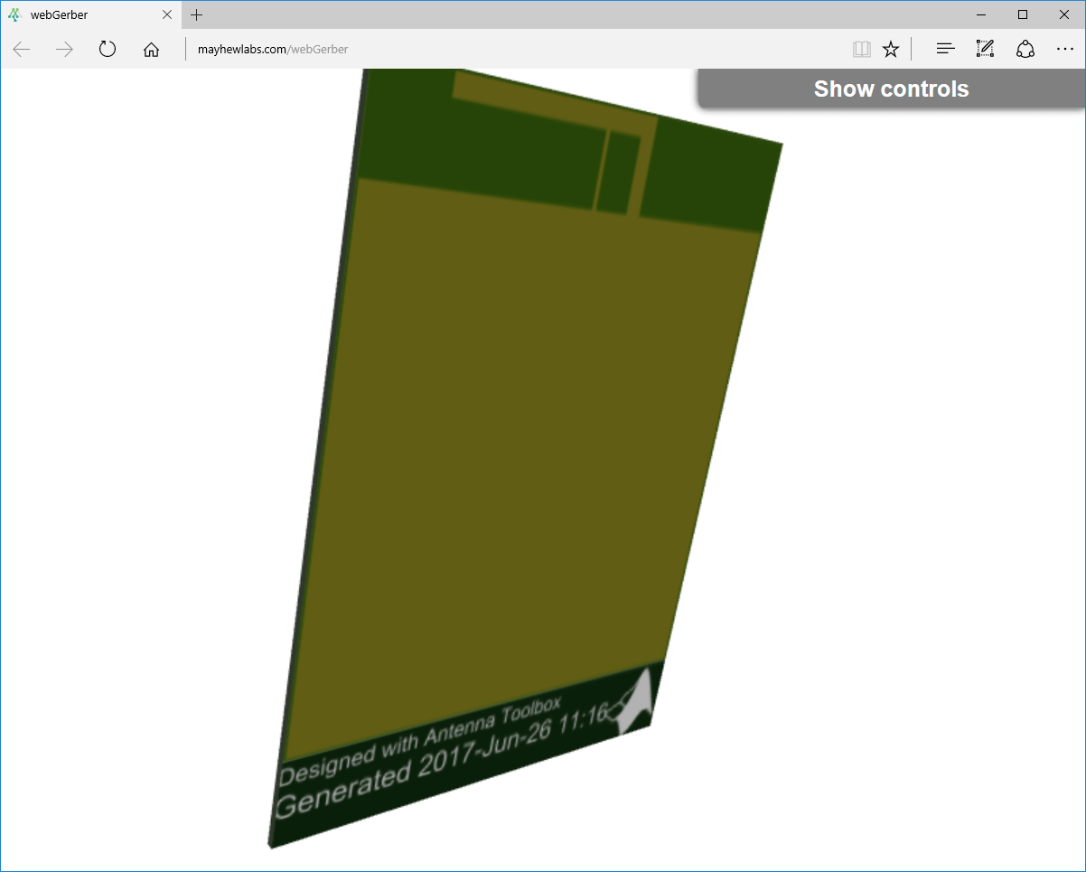
Click Done to view your Antenna PCB.

Version History
Introduced in R2017bThe PCBWriter object now allows you to enable or disable the watermark signature and connector labels in the Gerber files. Use the new:
EnableSignatureproperty to enable or disable watermark signature.EnableConnectorLabelproperty to enable or disable connector labels.
See Also
MATLAB Command
You clicked a link that corresponds to this MATLAB command:
Run the command by entering it in the MATLAB Command Window. Web browsers do not support MATLAB commands.
Web サイトの選択
Web サイトを選択すると、翻訳されたコンテンツにアクセスし、地域のイベントやサービスを確認できます。現在の位置情報に基づき、次のサイトの選択を推奨します:
また、以下のリストから Web サイトを選択することもできます。
最適なサイトパフォーマンスの取得方法
中国のサイト (中国語または英語) を選択することで、最適なサイトパフォーマンスが得られます。その他の国の MathWorks のサイトは、お客様の地域からのアクセスが最適化されていません。
南北アメリカ
- América Latina (Español)
- Canada (English)
- United States (English)
ヨーロッパ
- Belgium (English)
- Denmark (English)
- Deutschland (Deutsch)
- España (Español)
- Finland (English)
- France (Français)
- Ireland (English)
- Italia (Italiano)
- Luxembourg (English)
- Netherlands (English)
- Norway (English)
- Österreich (Deutsch)
- Portugal (English)
- Sweden (English)
- Switzerland
- United Kingdom (English)