Map Bus Data Types to a Register Interface
This example shows how to map bus data types to a register interface, generate an HDL IP core with a AXI4 Master interface, perform matrix multiplication in an HDL IP core, and write the output result to DDR memory. In this example, you:
Create a bus element by using bus creator blocks and map the bus element to an register interface such as AXI4-Lite and AXI4.
Generate an HDL IP core with AXI4 Master interface.
Access large matrices from the external DDR4 memory on the Xilinx Zynq Ultrascale+ MPSoC ZCU102 Evaluation Kit board using the AXI4 Master interface.
Perform matrix vector multiplication in the HDL IP core and write the output result back to the DDR memory using the AXI4 Master interface.
Requirements
For this example, you must have the following software and hardware installed and set up:
Xilinx Vivado Design Suite. To see the supported versions, see HDL Language Support and Supported Third-Party Tools and Hardware
Xilinx Zynq Ultrascale+ MPSoC ZCU102 evaluation kit.
HDL Coder Support Package for AMD FPGA and SoC Devices.
HDL Verifier™ Support Package for AMD® FPGA and SoC Devices.
Open the Model
This example models a matrix vector multiplication algorithm and implements it on the Xilinx Zynq FPGA board. Large matrices might not map efficiently to Block RAMs on the FPGA fabric. Instead, store the matrices in the external DDR memory on the FPGA board. The AXI4 Master interface can access the data by communicating with vendor-provided memory interface IP cores that interface with the DDR memory. This capability enables you to model algorithms that involve large data processing and require high-throughput DDR access, such as matrix operations, computer vision algorithms, and so on.
The matrix vector multiplication module supports fixed-point matrix vector multiplication with a configurable matrix size of 2 to 4000. The size of the matrix is run-time configurable through the AXI4 accessible register.
modelname = 'hdlcoder_axi_slave_bus_data_type';
open_system(modelname);
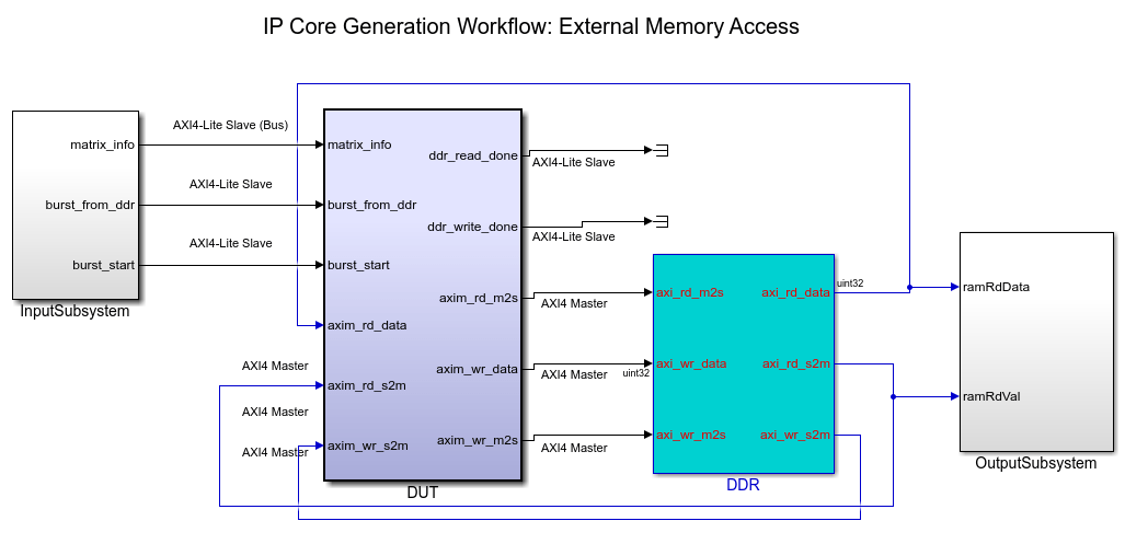
Use HDL Coder to generate a custom IP core that performs large matrix operations on FPGAs by using external memory. In MATLAB, type: hdladvisor('hdlcoder_axi_slave_bus_data_type/DUT')
Create Bus Element
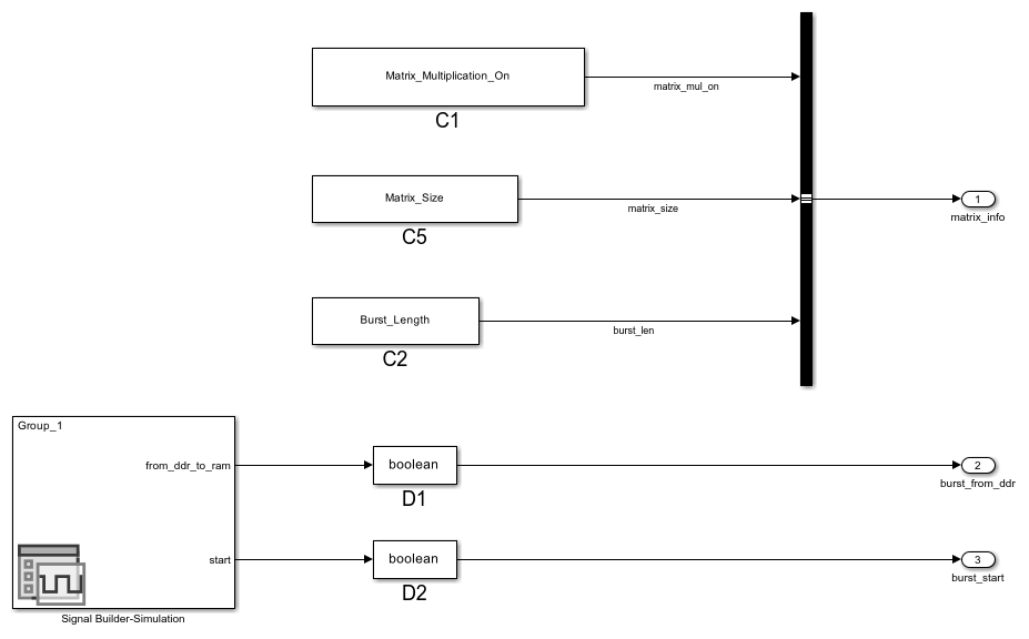
Use a Bus Creator block to combine the Matrix_Multiplication_On, Matrix_Size, and Burst_Length signals into a bus. For more information on the Bus Creator block, see Bus Creator
open_system('hdlcoder_axi_slave_bus_data_type/InputSubsystem')
Verify Simulation Results
You can simulate this example model and verify the simulation results by running this script in MATLAB:
hdlcoder_axi_slave_bus_data_type_simulation;
This script first initializes the parameters like Matrix_Size. By default, the Matrix_Size is 64, which generates a 64-by-64 matrix. This default value is kept small to ensure the model simulates faster. After the DUT is implemented on the FPGA board, the script uses a larger value for Matrix_Size because the FPGA calculation is much faster. You can also adjust these parameters in the script.
The script then simulates the model and verifies the result by comparing the logged simulation result to the expected value.
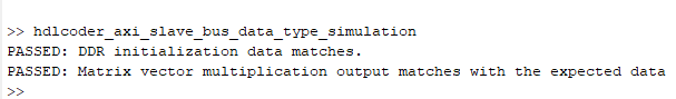
By default, the Matrix_Multiplication_On signal is true. The script verifies the matrix vector multiplication result.
When Matrix_Multiplication_On is false, the script verifies the loop back mode, which means that the DUT reads Burst_Length amount of data from DDR, and then writes the data back to DDR.
Generate HDL IP Core with AXI4 Master Interface
Next, start the HDL Workflow Advisor and deploy the DUT on the Zynq hardware. For a more detailed step-by-step guide, see Get Started with IP Core Generation from Simulink Model example.
1. Set up the Xilinx Vivado synthesis tool path using hdlsetuptoolpath command. Use your own Vivado installation path when you run the command. In the MATLAB Command Window, enter:
hdlsetuptoolpath('ToolName', 'Xilinx Vivado', 'ToolPath', vivadopath)
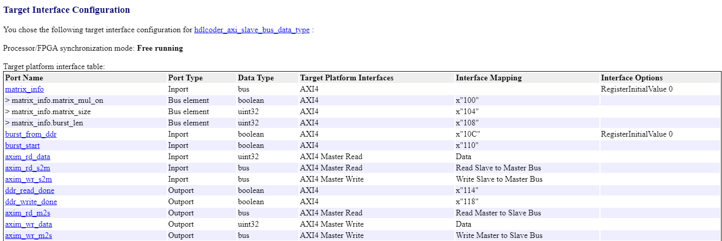
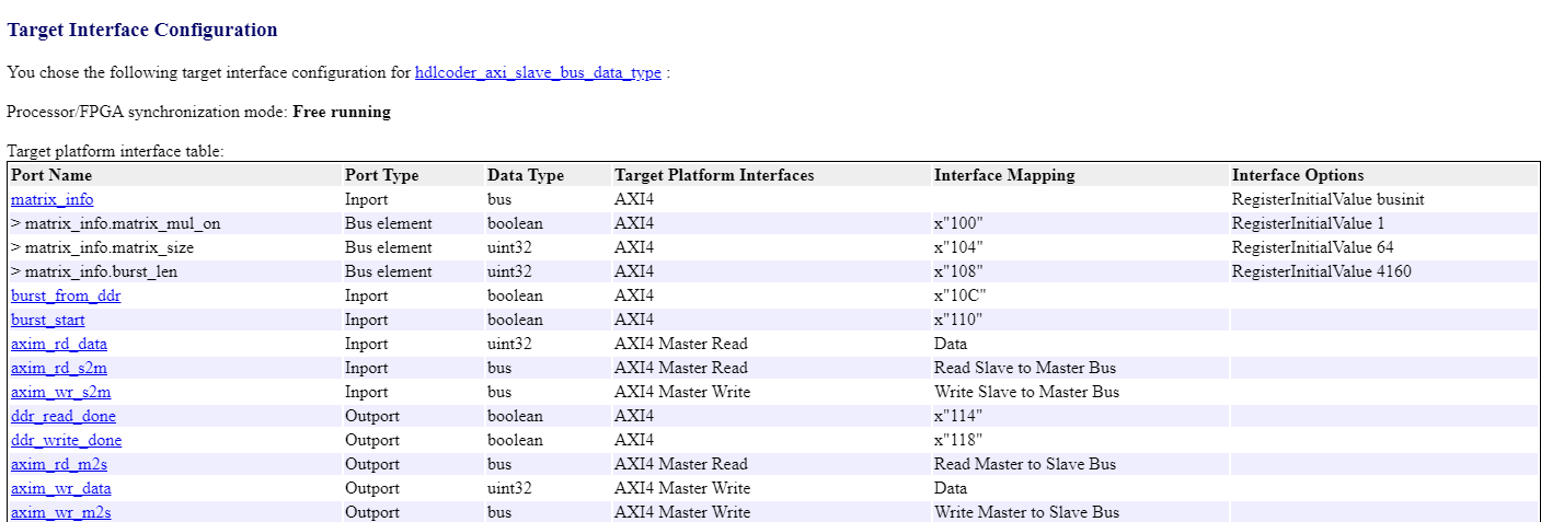
2. Start the HDL Workflow Advisor from the DUT subsystem hdlcoder_axi_slave_bus_data_type/DUT. The target interface settings are saved in the model. The Target workflow parameter is IP Core Generation, and the Target platform parameter is Xilinx Zynq Ultrascale+ MPSoC ZCU102 Evaluation Kit. The Reference Design parameter is |Default System with External DDR4 memory access. This image shows the Target platform interface table settings.
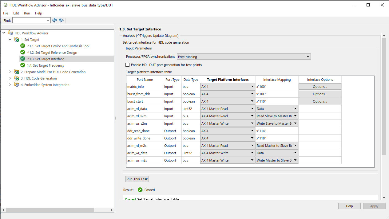
In this example, the bus data type ports such as matrix_info and input parameter ports such as burst_from_ddr and burst start are mapped to the AXI4 interface. HDL Coder generates the AXI4 interface-accessible registers for these ports. Later, you can use MATLAB to tune these parameters at run time when the design is running on the FPGA board.
You can specify the bus data type initial values in the Target platform interface table by specifying either the initial values or by creating a variable to store the initial values in a structure and using the variable name in the Set Interface Options window. To specify the initial value, click Options under the Interface Options column in the Target platform interface table.
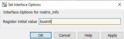
Alternatively, specify the initial values in the Set Interface Options window.
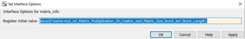
To store the bus data type initial values in a variable called businit, run this code:
businit = struct('matrix_mul_on',Matrix_Multiplication_On,'matrix_size',Matrix_Size,'burst_len',Burst_Length)
Then specify the businit variable in the Set Interface Options window.
The AXI4 Master interface has separate read and write channels. The read channel ports such as axim_rd_data, axim_rd_s2m, axim_rd_m2s are mapped to the AXI4 Master Read interface. The write channel ports such as axim_wr_data, axim_wr_s2m, axim_wr_m2s are mapped to the AXI4 Master Write interface.
3. Right-click Generate RTL Code and IP Core and select Run to Selected Task to generate the IP core. You can find the register address mapping and other documentation for the IP core in the generated IP core report.
The report shows the individual bus elements and their address mappings.
If you specify the initial value for the bus element using the businit variable, the generated IP core report shows the bus element initial values.
4. Right-click Build FPGA Bitstream and select Run to Selected Task to generate the Vivado project. Build the FPGA bitstream.
During the project creation, the generated DUT IP core is integrated into the Default System with External DDR4 Memory Access reference design. This reference design comprises of a Xilinx Memory Interface Generator IP that communicates with the onboard external DDR4 memory on the ZCU102 platform. The AXI Manager IP is also added to enable MATLAB to control the DUT IP and to initialize and verify the DDR memory content.
Run FPGA Implementation on Xilinx Zynq Ultrascale+ MPSoC ZCU102 Evaluation Kit
After the FPGA bitstream is generated, run the Program Target Device task to program the FPGA board through the JTAG cable.
You can then run the FPGA implementation and verify the hardware result by running this script in MATLAB:
hdlcoder_axi_slave_bus_data_type_hw_run_ZCU102.m
This script first initializes the Matrix_Size variable to 2000, which generates a 2000-by-2000 matrix. You can adjust the Matrix_Size up to 4000.
The script then configures the AXI4 Master read and write channel base addresses. These addresses define the base address that the DUT reads from the external DDR memory, and then writes to external DDR memory. In this script, the DUT reads from base address '80000000' and writes to the base address '90000000'.
The AXI Manager initializes the external DDR4 memory with input vector and matrix data and clears the output DDR memory location.
The DUT calculation starts by controlling the AXI4 accessible registers. The DUT IP core reads input data from the DDR memory, performs the matrix vector multiplication, and then writes the result back to the DDR memory.
The output result is read back to MATLAB and compared to the expected value. The hardware results are verified in MATLAB.
