DVB-S2 Receive Using AMD RFSoC Device
This example shows how to simulate and deploy a Digital Video Broadcast Satellite Second generation (DVB-S2) receive algorithm in Simulink® using an SoC Blockset™ implementation targeted on an AMD® Zynq® UltraScale+™ RFSoC ZCU111 evaluation board. Using this example, you can integrate DVB-S2 HDL Receiver (Wireless HDL Toolbox) example into the SoC Blockset implementation. This example shows how to measure the bit error rate (BER) of a DVB-S2 link using impairments introduced on the hardware.
Supported Hardware Platforms
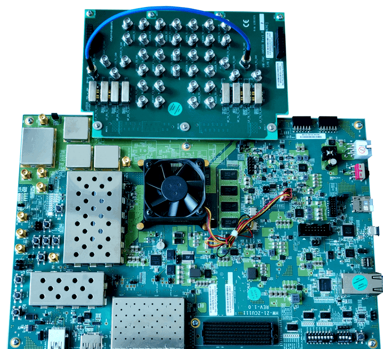
AMD Zynq UltraScale+™ RFSoC ZCU111 evaluation kit + XM500 Balun card
Design Task
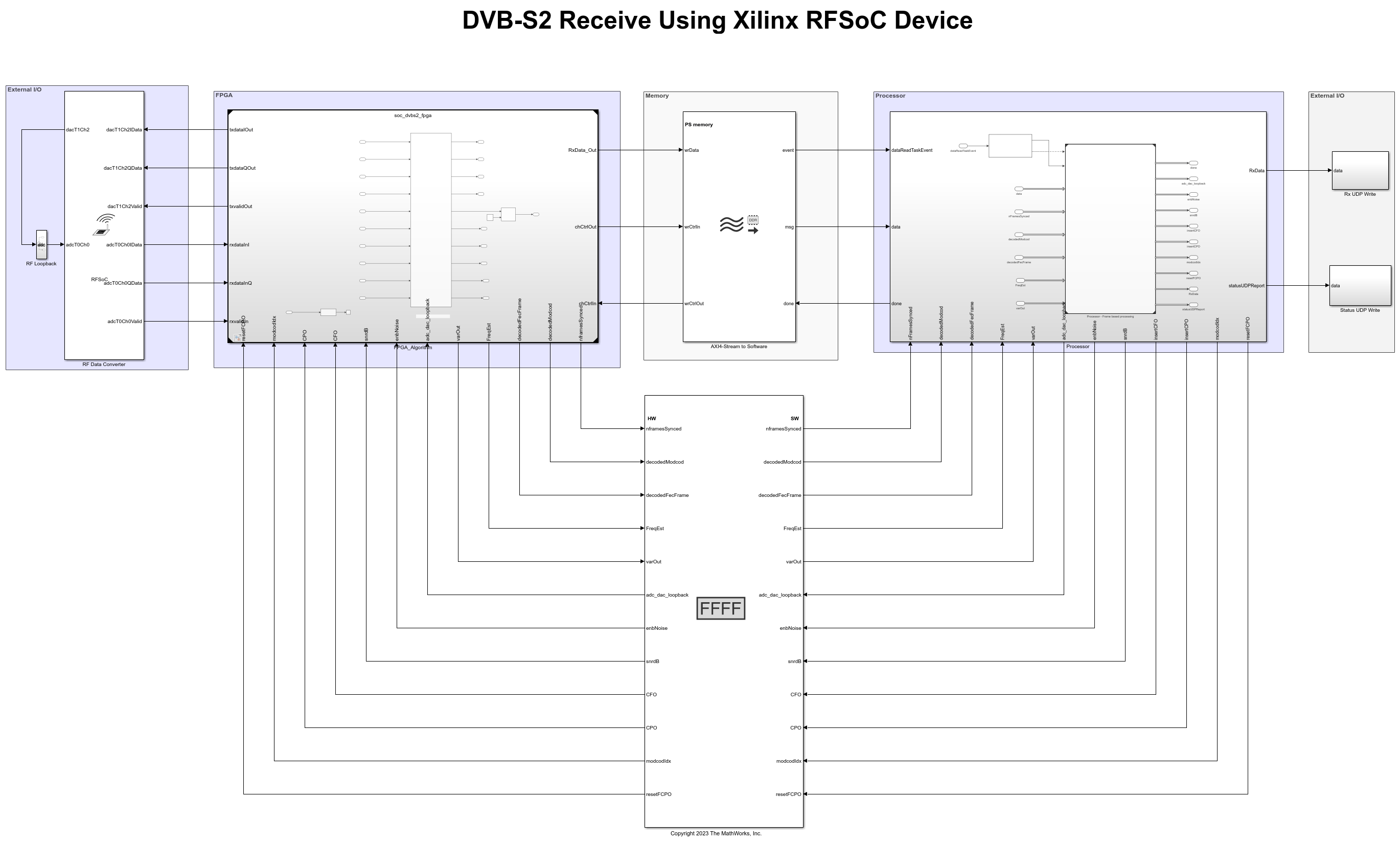
In this example, the design task is to build a DVB-S2 receiver and implement the system on an AMD RFSoC device. This example shows the workflow for designing, simulating, and deploying the DVB-S2 receive algorithm on the hardware. This figure shows the conceptual overview of the example.

The DVB-S2 Receiver block performs high-speed signal processing tasks and make the DVB-S2 receive algorithm well suited for FPGA implementation on the programmable logic (PL) of the radio platform. To implement this algorithm on the PL, the example uses the Simulink® hardware model from the DVB-S2 HDL Receiver (Wireless HDL Toolbox) example. The example is also equipped with an internal channel to apply carrier frequency offset (CFO), carrier phase offset (CPO), and an HDL additive white Gaussian noise (AWGN) channel from the HDL Implementation of AWGN Generator (Wireless HDL Toolbox) example. Control signals CFO, CPO and snrdB are provided to tune the channel.
Design Using SoC Blockset
Create an SoC model soc_dvbs2_top as the top model and set the Hardware Board to Xilinx Zynq UltraScale+ RFSoC ZCU111 evaluation kit. The top model includes FPGA model soc_dvbs2_fpga and processor model soc_dvbs2_proc, which are instantiated as model references. The top model also includes AXI4-Stream to Software block that shares the external memory between the FPGA and the processor.
Create an SoC model soc_dvbs2_hwtop as the top model for the simulation of a hardware algorithm with a static configuration. This model includes the FPGA model soc_dvbs2_fpga.
RF Data Converter Configuration
An RFSoC device has its RF data converter connected to the PL. To configure the analog to digital converter (ADC) and digital to analog converter (DAC) settings, use the RF Data Converter block. The block provides an interface to the AMD RF Data Converter IP in Simulink to model a wireless system destined for implementation on an AMD RFSoC device.
To meet the system requirements of a 860 MHz RF carrier frequency and 4 Msps baseband sample rate, configure the RF Data Converter block according to the settings described here and shown in the figure.
Set the NCO frequency parameter for the DAC and ADC mixers to
0.860GHz.Set the DAC and ADC sample rate to
2048MSPS.Choose the values of Interpolation mode (xN), Decimation mode (xN), and Samples per clock cycle parameters such that the effective clock cycle (sample rate) for the wireless algorithm FPGA is the desirable value. For this example, the desired value is 128 Msps. This value is calculated and displayed on the block mask as the Stream clock frequency (MHz) parameter after you click Apply.
Set the Decimation mode (xN) parameter to
4. The effective sample rate after decimation is 512 Msps.Set the Samples per clock cycle parameter to
4to get the clock cycle (baseband sample rate) to 128 Msps.
Similarly, in the DAC tab, set the Interpolation mode (xN) parameter to 4 and the Samples per clock cycle parameter to 4. With these settings, the Stream clock frequency parameter is 2048/(4*4) = 128 MHz

Hardware Logic Design
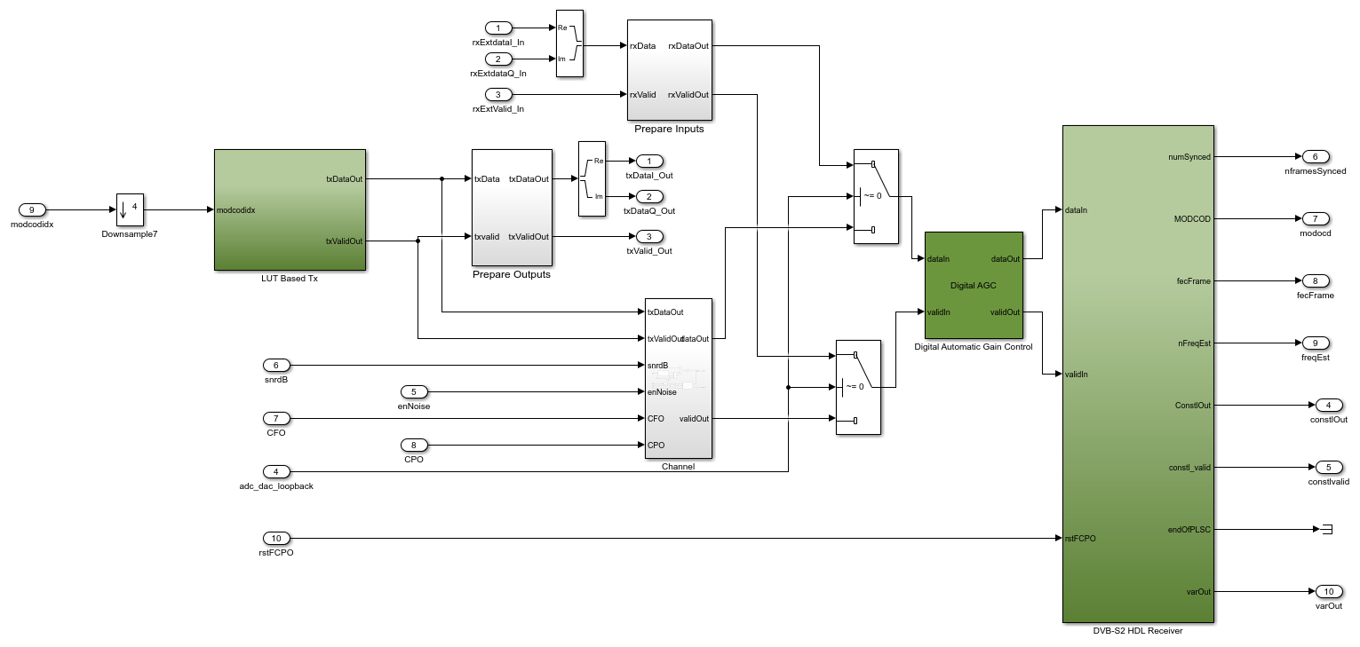
The FPGA model soc_dvbs2_fpga contains three subsystems: Vector Interpolation (which is connected to the DAC portion of the RFDC block), Vector Decimator (which is connected to the ADC portion of the RFDC block), and DVBS2 TxRx.
The Vector Decimator subsystem receives the packed four samples as 64 bits. The Vector Decimator subsystem decimates input vector samples by 4 and sends them to the DVBS2 TxRx subsystem. The sample rate after the Vector Decimator block is 128 Msps, as expected by DVBS2 TxRx subsystem for its processing.

The DVBS2 TxRx subsystem comprises an LUT Based Tx, DVB-S2 HDL Receiver, Channel, Digital Automatic Gain Control, Prepare Inputs, and Prepare Outputs subsystems.
The
LUT Based Txstores the short DVB-S2 Frames corresponding to all the supported MODCOD values. These frames are passed through a root raised cosine(RRC) filter using Discrete FIR Filter (DSP HDL Toolbox) block. The interpolation filters convert the DVB-S2 waveform from a baseband sample rate of 4 Msps to 128 Msps.
The
DVB-S2 HDL Receiversubsystem is implemented from the DVB-S2 HDL Receiver (Wireless HDL Toolbox) example.
The
Channelsubsystem has aWhite Gaussian Noise Generatorsubsystem and an NCO (DSP HDL Toolbox) block. The White Gaussian Noise Generator has an AWGN generator from the HDL Implementation of AWGN Generator (Wireless HDL Toolbox) example. The NCO block performs CFO insertion.
In the receive path, the Vector Decimator subsystem receives the four samples with a sample rate of 128 Msps from the RF Data Converter block. The Vector Decimator subsystem decimates input vector samples by 4 and sends them to the DVB-S2 HDL receiver. The sample rate after the Prepare Inputs subsystem is 16 Msps, as expected by the DVB-S2 HDL Receiver subsystem for its processing. The DVB-S2 HDL Receiver subsystem sends the processed data to the processor with a sample rate of 128 MHz. In the transmit path, the LUT Based Tx subsystem sends the samples to the RF Data Converter block through the Vector Interpolation subsystem. The Vector Interpolation block interpolates the input samples by 32 (128 Msps) and sends them to the RF Data Converter block as a vector of four samples.
Processor Logic Design
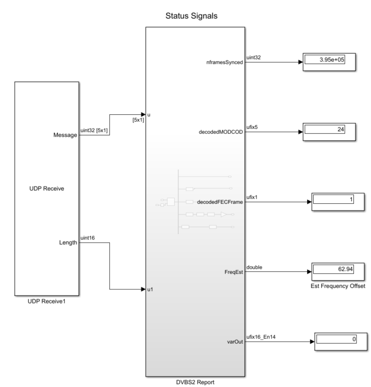
The processor logic contains a read task and a periodic task. The periodic task is a timer-driven task with a periodic time of 1e-3, which is defined in the task manager. The periodic task drives the control and status signals of the DVB-S2 hardware algorithm through the AXI4-Lite registers. The model displays status information such as number of frames synchronized, estimated frequency offset, decoded MODCOD, decoded FECFRAME, BB Header parameters: User Packet Length (UPL), DFL, SYNC and TSorGS, and number of bits received and bits errored from the DVB-S2 receiver. The controller provides the constellation data and status information to the MATLAB host by using UDP blocks. The RxUDPData and StatusUDPData subsystems relay the constellation and status signals, respective to the host over the UDP protocol.
The read task is an event-based task driven by the arrival of data from the FPGA through DDR memory. This data comprises the constellation data of the selected MODCOD. The previous two tasks are modeled under the Processor Algorithm Wrapper subsystem in processor model soc_dvbs2_proc and are connected to the Task Manager block at the top level.

Host Model
The processor sends the DVB-S2 HDL Receiver subsystem outputs data and receiver status signals directly back to the host over the Ethernet link by using UDP Write blocks. The IP address of the UDP Write block in the processor model must be configured to the IP address of the host. This interface model, which runs on the host, shows how to receive data from the hardware platform and how to postprocess it.
Simulate
To confirm its basic operation, run the hardware generation model using LUT based DVB-S2 transmitter. The model callback runs the soc_dvbs2_init initialization script. To access the callback initialization, select MODELING > Model Settings > Model Properties > Callbacks > InitFcn.
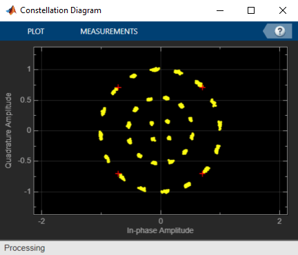
Because the model contains a large number of HDL-optimized blocks, which simulates using sample-based signals it takes a while for the simulation. The figure shows the constellation diagram from the simulation.
To enable the AWGN channel between the LUT Based Tx subsystem and DVB-S2 HDL Receiver subsystem, set adc_dac_loopback to false. You can control the channel by using channel impairment controls CFO, CPO and snrdB. When you set adc_dac_loopback to true, the DVB-S2 signals are received externally through the ADC, DAC, and RF Data converter. The channel impairments are added externally in real time.
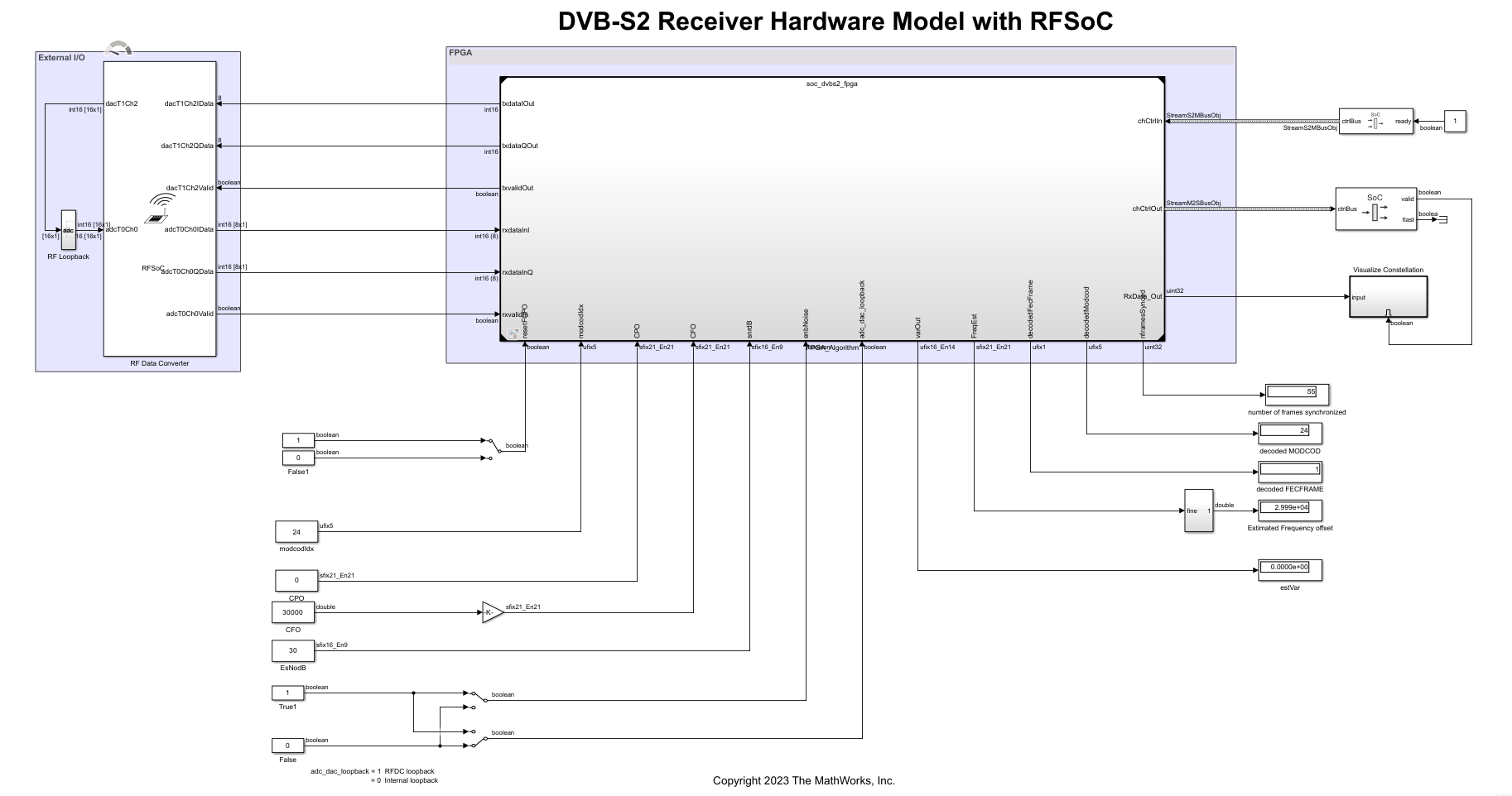
If you want to see the complete hardware and software simulation of the DVB-S2 receive algorithm and the controller dynamic configuration, run the soc_dvbs2_top model. Run the host model to see the receiver status signals and constellation diagram.

Note
Coarse frequency offset is now disabled and considered for further exploration on the targeting side. The model can now handle carrier drifts less than 5% of symbol rate using fine frequency synchronization. The synchronization is averaged over 512 pilot blocks to estimate the fine frequency offset as explained in the DVB-S2 HDL PL Header Recovery (Wireless HDL Toolbox) example. Consequently, the simulation time is increased.
To enhance hardware stability, data recovery is only enabled once synchronization is complete. For initial synchronization, the model sets the MODCOD value to '0', which can slow down simulations for header decoding parameters. To improve simulation speed, disable the "Force MODCOD to 0 during initial synchronization" parameter in the Synchronizer and PL Header Decoder subsystem block mask. However, for hardware deployment, it is recommended to enable this parameter to prevent instability during data decoding.
Implement and Run on Hardware
Hardware Setup
Connect the SMA connector on the XM500 Balun card to complete the loopback between the DAC and ADC, according to these connections: DAC229_T1_CH2 (J5) to ADC224_T0_CH0 (J4).
To implement the model on a supported SoC board, use the SoC Builder tool. Ensure that the Hardware Board option is set to Xilinx Zynq UltraScale+ RFSoC ZCU111 Evaluation Kit on the System on Chip tab of the Simulink Toolstrip.
To open SoC Builder, click Configure, Build, & Deploy. After the SoC Builder tool opens, follow these steps.
On the Setup screen, select Build Model and click Next.
On the Review Memory Map screen, click View/Edit Memory Map to view the memory map and then click Next.
On the Select Project Folder screen, specify the project folder and then click Next.
On the Select Build Action screen, select Build External mode and then click Next.
On the Validate Model screen, click Validate to check the compatibility of the model for implementation and then click Next.
On the Build Model screen, click Build to begin building the model. An external shell opens when FPGA synthesis begins. Click Next.
On the Connect Hardware screen, click Test Connection to test the connectivity of the host computer with the SoC board. Click Next to go to the Run Application screen.
FPGA synthesis can take more time to complete. To save time, you can use the provided pregenerated bitstream by following these steps.
Close the external shell to terminate FPGA synthesis.
Copy the pregenerated bitstream to your project folder by entering this command at the MATLAB command prompt.
copyfile(fullfile(matlabshared.supportpkg.getSupportPackageRoot,...
'toolbox','soc','supportpackages','whdlsocexamples','bitstreams',...
'soc_dvbs2_top-XilinxZynqUltraScale_RFSoCZCU111EvaluationKit.bit'),...
'./soc_prj');
Click Load and Run to load the pregenerated bitstream and run the model on the SoC board. After the bit file is loaded, open the generated software model.

Run the model in external mode by clicking Monitor & Tune. You can control the configuration from the Simulink model.
Constellation and Status Signals from Hardware
Run the host model to see the received constellation data and receiver status signals. When the host interface model runs successfully, the model displays the constellation diagram and status signals for the case MODCOD 24.
Further Exploration
This example demonstrated how to integrate the DVB-S2 receive algorithm on an AMD ZCU111 evaluation board using an SoC Blockset implementation. This example return the decoded data and evaluates the Bit error rate (BER) of the DVB-S2 receiver design from the hardware. This example does not use the radio frequency (RF) card in the transceiver loop. Using the Transmit and Receive Tone Using OTAVA DTRX2 mmWave Radio Card example, you can integrate an OTAVA DTRX2 mmWave radio card with a Xilinx® Zynq® UltraScale+™ RFSoC ZCU208 Evaluation Kit by using SoC Blockset™. The DVB-S2 system then receives the data back into the FPGA by using the OTAVA DTRX2 and RFDC blocks and evaluates the Over the Air (OTA) received BER.
In this example, DVB-S2 Transmitter is designed using an LUT-based approach and it supports only short frames. However, you can replace the functionality of the transmitter in this example with DVB-S2 HDL Transmitter (Wireless HDL Toolbox) example, which works for both FEC frame types. You can configure the model for the FECFrame type normal and short through the soc_dvbs2_init script. You cannot change this script dynamically. However, the DVB-S2 blocks such as DVB-S2 LDPC Decoder (Wireless HDL Toolbox), DVB-S2 BCH Decoder (Wireless HDL Toolbox), and DVB-S2 Symbol Demodulator (Wireless HDL Toolbox) are capable of handling FEC frame, code rate and modulation type through input ports. Therefore, you can modify the model by enabling these options in the receiver.
See Also
Topics
- DVB-S2 HDL Receiver (Wireless HDL Toolbox)