Hardware-Software Co-Design Workflow
This guide helps you to deploy partitioned hardware-software (HW/SW) co-design implementations of SDR algorithms for Xilinx® Zynq®-based radio hardware.
You can use Simulink® to design, simulate, and verify your application, and to perform what-if scenarios to optimize performance. Then you can decide which system elements to implement on the programmable logic, and which system elements run on the ARM® processor.
Using this workflow, you can automatically generate HDL code for the programmable logic using HDL Coder™, and generate C code for the ARM processor using Embedded Coder®. Finally, you can implement the design on the radio hardware.
This workflow uses the HW/SW Co-Design QPSK Transmit and Receive Using Analog Devices AD9361/AD9364 example as a reference design.
Step 1: Verify Radio Hardware Connection
Follow the instructions in Installation for Hardware-Software Co-Design. Make sure that all support packages and third-party tools required by the HW/SW co-design workflow are installed and configured.
Create a radio object by using the
sdrdevfunction. If you are using and FMCOMMS5 radio hardware, specify'FMCOMMS5'instead of'AD936x'when callingsdrdev.radio = sdrdev('AD936x');Before you can use the HW/SW co-design workflow, the host computer must be communicating with the radio hardware. Verify host-radio communication by calling the
testConnectionfunction on the radio object. This function queries the device and returns a logical value to indicate either success or failure.testConnection(radio);
Step 2: Set Up Third-Party Tools
Set up your system environment to access Xilinx
Vivado® from MATLAB®. The hdlsetuptoolpath function adds the required
folders to the MATLAB search path, using the Xilinx installation folder that you specify.
For example, use this code to set up your system environment for Windows® machines.
hdlsetuptoolpath('ToolName','Xilinx Vivado','ToolPath', ...
                'C:\Xilinx\Vivado\2024.1\bin\vivado.bat')
For example, use this code to set up your system environment for Linux® machines.
hdlsetuptoolpath('ToolName','Xilinx Vivado','ToolPath', ...
                 '/opt/Xilinx/Vivado/2024.1/bin')
Step 3: Create Algorithm and Partition the Design
When partitioning an SDR algorithm, use the ARM processor for slower-rate control functionality, and use the FPGA fabric for high-rate signal processing. Group the blocks you want to implement on programmable logic into an atomic subsystem. This subsystem is the boundary of your hardware-software partition. The blocks inside this subsystem are implemented on programmable logic, and the blocks outside this subsystem are used to verify its operation. The blocks around the subsystem can contain the algorithm that you eventually implement on the ARM processor.
For example, in HW/SW Co-Design QPSK Transmit and Receive Using Analog Devices AD9361/AD9364, the QPSK transmit-and-receive physical layer front ends are implemented on the programmable logic. These layers include high-rate operations such as gain control, filtering, and frequency compensation. The data encoding and decoding are lower rate and are implemented on the ARM processor, which outputs the decoded message to a console window.
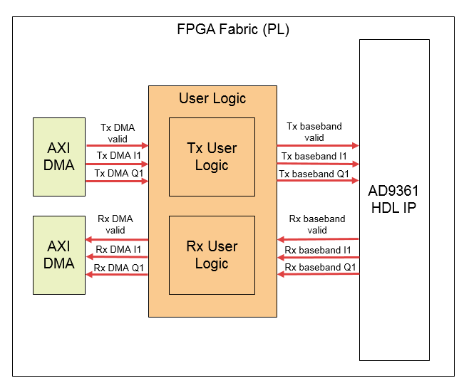
The workflow has specific requirements for the boundary between the hardware and software. The following diagram shows the mandatory data and valid user logic inputs and outputs for a single-channel transmit-and-receive reference design. Multiple-channel reference designs contain multiple sets of I and Q data lines. Transmit-only or receive-only reference designs contain only transmit or receive signals.
Guidelines
Each data input or output must be 16 bits. Complex inputs and outputs are not supported at the ports of the HDL subsystem. Therefore, real and imaginary signals must be modeled at the subsystem boundaries.
The diagram shows only single-channel inputs and outputs. You can also choose multiple channels. For an overview of the number of channels you can use in each supported hardware, see Channel I/O. Each channel consists of a real and an imaginary part.
Model all the ports for a given reference design, even when the ports are not used.
The data inputs and outputs to the subsystem are modeled using separate data and valid signals. In Simulink, the data and valid lines must be driven at the same sample rate. Therefore, the input and output clock rates of the subsystem must be equal.
Clock the data and valid signals at the fastest rate of the HDL subsystem. When the
Tx-baseband-validsignal is de-asserted, the last sample value is held.You can clock the AXI4-Lite register ports at arbitrary rates.
You can add AXI4-Stream input and output ports to connect to separate DMA engines from those shown above. You can use these ports to move data to the processing system via the AXI4-Stream IIO Read and AXI4-Stream IIO Write blocks from the Embedded Coder Support Package for AMD SoC Devices. For an example, see HW/SW Co-Design with AXI4-Stream Using Analog Devices AD9361/AD9364.
Step 4: Generate HDL IP Core Using HDL Workflow Advisor
HDL IP core generation enables you to generate a shareable and reusable IP core module from a Simulink model automatically. The generated IP core connects to an embedded processor, such as the ARM processor on the radio hardware. HDL Coder generates HDL code from the Simulink blocks. It also generates HDL code for the AXI interface logic connecting the IP core to the embedded processor. By using an SDR reference design, you can create an IP core that integrates into the radio hardware. Using this core, you can configure the RF card and send and receive data.
After you are satisfied with the simulation behavior of the hardware subsystem, generate the HDL IP core and integrate it with the SDR reference design.
A. Start HDL Workflow Advisor
Right-click the subsystem and select HDL Code > HDL Workflow Advisor.
B. Select Workflow and Synthesis Tool
At Workflow Advisor Step 1.1, select IP Core Generation
for the Target workflow. Then select the required
Zynq radio hardware for the Target platform. You can
choose one of the following platforms:
ADI RF SOM
ZedBoard and FMCOMMS2/3/4
ZC706 and FMCOMMS2/3/4
ZC706 and FMCOMMS5
ZCU102 and FMCOMMS2/3/4
Finally, select Xilinx Vivado as the
Synthesis tool.
Click Run This Task.
C. Select and Configure Reference Design
At Workflow Advisor Step 1.2, select the reference design for your system:
Receive pathTransmit pathReceive and transmit pathTransmit path with Deep Learning Processor(since R2026a)Receive path with Deep Learning Processor(since R2026a)Receive and transmit path with Deep Learning Processor(since R2026a)
Click Run This Task.
At Workflow Advisor Step 1.3, set the target interface and verify that Processor/FPGA synchronization is set to
Free running. Then map your user logic to the reference design. When mapping the RF channels, each I and Q component refers to a 16-bit port on the user logic. The number defines the channel designation. For example,Baseband Rx I1 In [0:15]maps to the real part of the receiver for channel 1 on the RF card. The following diagram shows the target platform interfaces for the QPSK transmit-and-receive reference design with two AXI4-Lite registers.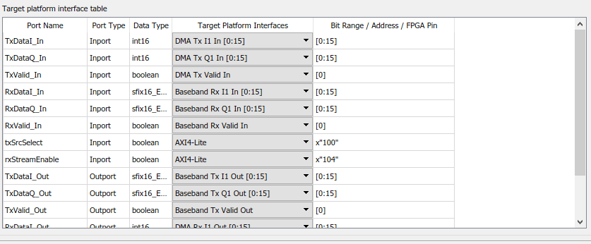
Click Run This Task. Check for warnings in the log text area at the bottom of the Workflow Advisor and make the required changes before proceeding.
Warning
Direct Inport to Outport passthrough is not supported. If you connect an Inport directly to an Outport, you must place a delay in the path.
At Workflow Advisor Step 1.4, choose the synthesis frequency for your design. The synthesis frequency provides the FPGA bitstream generation tools with a target clock rate for user logic synthesis. You can check the sample times for your model by selecting Debug > Information Overlays > Sample Time > Legend. Your user logic synthesis frequency must be greater than or equal to the highest sampling frequency in the HDL subsystem. The default synthesis frequency is 61.44 MHz, which is the fastest sample rate supported by the SDR hardware. The minimum clock rate is 520.834 kHz, which is the lowest sample rate supported by the SDR hardware.
Click Run This Task.
D. Run Design Checks
Workflow Advisor Step 2 prepares the design for generation by performing design checks. Click Run This Task.
E. Generate HDL IP Core
Workflow Advisor Step 3 performs the HDL code generation for the IP core. Click Run This Task.
Step 5: Integrate IP Core into Xilinx Vivado Project
Workflow Advisor Step 4.1 integrates the IP core into the SDR reference design and generates a Vivado project. Click Run This Task.
Step 6: Generate Software Interface Model and Library
Workflow Advisor Step 4.2 generates a Zynq software interface model and a software interface library. The library contains the blocks that you use to generate your own software interface model. The software interface model outlines how to create a user application model and guides you in specifying the sampling rates for the receiver. Click Run This Task.
Software Interface Library
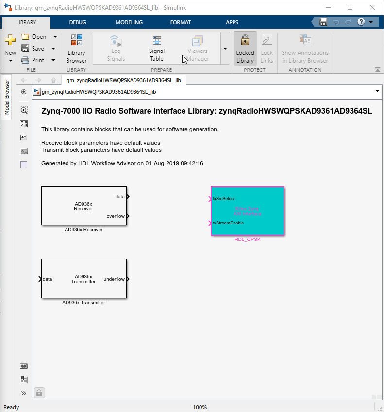
The library contains the AXI Interface block generated from the subsystem in the QPSK example. The block exposes only the AXI-lite control ports and not the data ports. The data ports are present on the Receiver and Transmitter blocks. These blocks represent the data interface between the fabric HDL user logic and the ARM. They contain the means to configure the RF chip. If you use the library blocks in your downstream models, updates that you make to your HDL subsystem propagate to this library automatically. Then, when you run through the workflow, the updates propagate to your software generation models. When using the library blocks, make sure that you configure the parameters as required by your application.
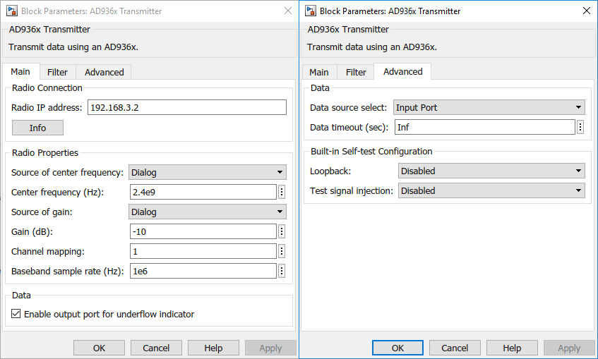
Generated Transmitter. The generated transmitter block contains radio transmitter properties and a
timeout value for frame transfer completion. The default timeout is
Inf seconds.
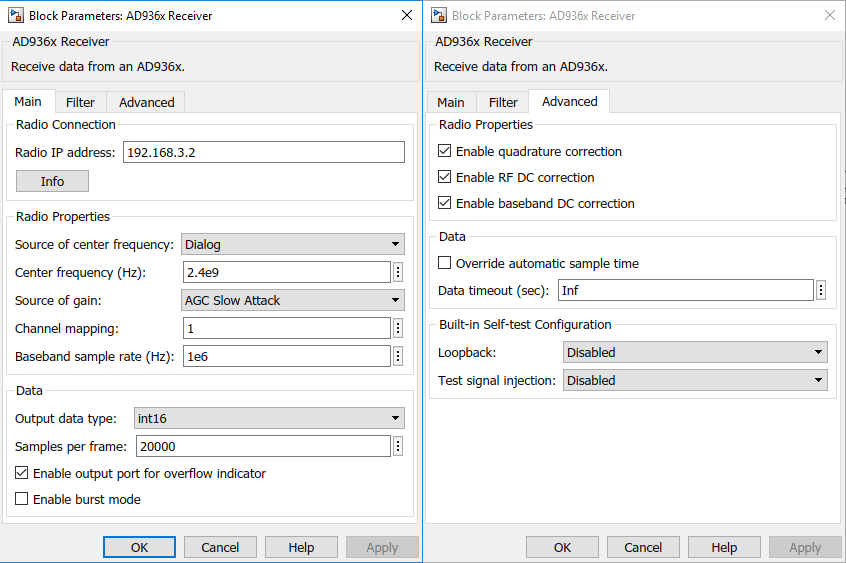
Generated Receiver. The generated receiver block contains radio receiver properties and a timeout
value for frame transfer completion. The default timeout is Inf
s.
Software Interface Model
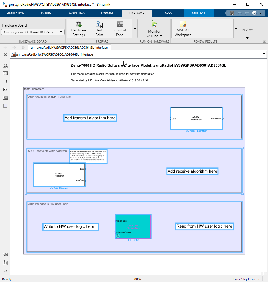
You can use the generated software interface model as a starting point for full software targeting to the Zynq, including external mode simulation, processor-in-the-loop, and full deployment. This model is overwritten each time you run Step 4.2. Save this model under a unique name and develop your software algorithm in your saved model.
When you include AXI4-Stream interfaces, the AXI4-Stream driver blocks are not automatically generated. You must add the AXI4-Stream IIO Read and AXI4-Stream IIO Write driver blocks from Simulink Library Browser > Embedded Coder Support Package for AMD SoC Devices library to your model. Before you generate code from the software interface model, you must configure the AXI4-Stream IIO Read and AXI4-Stream IIO Write driver blocks by following the steps outlined in the Generate IP Core with an AXI4-Stream Interface (HDL Coder).
The model shows the generated software interface model from the QPSK example.
Step 7: Generate FPGA Bitstream and Program Zynq Hardware
Generate the bitstream.
Workflow Advisor Step 4.3 generates a bitstream for the FPGA fabric.
To keep using MATLAB while the FPGA image builds, select Run build process externally to generate the bitstream in an external shell. The step completes in several minutes, after basic project checks have been performed and the step is marked with a green check mark. Before continuing, verify in the Command Window that the Vivado bitstream built without printing an error.
Program the Zynq hardware.
Workflow Advisor Step 4.4 downloads the bitstream onto the device.
Before continuing with this step, call the
zynqfunction with the following syntax to make sure that MATLAB is set up with the correct physical IP address of the radio hardware.By default, the physical IP address of the radio hardware is 192.168.3.2. If you alter the radio hardware IP address during the hardware setup process, you must supply that address instead.devzynq = zynq('linux','192.168.3.2','root','root','/tmp');
In Workflow Advisor Step 4.4, you have three options to download the bitstream.
With
Download, the bitstream is persistent across power cycles (recommended).With
JTAG, the bitstream is not persistent across power cycles
Alternatively, if you want to load the bitstream outside Workflow Advisor, call the
downloadImagefunction. If you are using and FMCOMMS5 radio hardware, specify'FMCOMMS5'instead of'AD936x'when callingsdrdev.radio = sdrdev('AD936x'); downloadImage(radio,'FPGAImage',... 'hdl_prj\vivado_ip_prj\vivado_prj.runs\impl_1\system_top.bit')
This function call renames the generated
system_top.bitfile tosystem.bitand downloads the file over an Ethernet connection to the radio hardware. This bitstream is persistent across power cycles.
Step 8: Configure Software Interface Model
To configure the software interface model, set up parameters according to the application you are modeling.
The following procedure shows how to configure one specific application. If your application requires different settings, see Guidelines for Configuring the Software Interface Model.
On the Hardware tab, in the Hardware Board section, select one of these options depending on your target platform:
Xilinx Zynq UltraScale+ MPSoC ZCU102
                              IIO Radio
for the ZCU102 and FMCOMMS2/3/4 target platformXilinx Zynq-7000 Based IIO Radiofor any of these platforms:ADI RF SOM
ZedBoard and FMCOMMS2/3/4
ZC706 and FMCOMMS2/3/4
ZC706 and FMCOMMS5
Note that the Hardware Board is automatically set depending on the target platform chosen in Step 4.B.
Configure the QPSK transmit-and-receive model to run with the Base rate trigger parameter set to
Transmitter interrupt.Configure the width of the input vector (the transmit frame size) to a value that meets your application requirements.
Connect the underflow port to a Stop Simulation block. An underflow implies an interruption in the data being sent, which is an error in a continuously streaming example.
In the Receiver block, set the Samples per frame parameter to a value that meets your application requirements, for example,
DataFrameLength/2. Then set the Data timeout (sec) parameter to a value that is smaller than the frame rate, for example,200e-6.To qualify valid data that enters the receiver model, connect the data valid port to an enabled subsystem.
Connect the overflow port of the Receiver block to a Stop Simulation block. Overflow implies an interruption in the data being sent, which is an error in a continuously streaming example.

Step 9: Run on ARM Processor Using External Mode
You can use external mode in Simulink to tune the algorithm you develop when it runs on the hardware. First you deploy the algorithm to the ARM processor in the Zynq board. Then you link the algorithm with the Simulink model on the host computer through the Ethernet connection. The main role of the Simulink model is to tune and monitor the algorithm running on the hardware. Because the ARM processor is connected to the HDL IP core through the AXI interface, you can use external mode to tune and monitor the hardware.

To run the algorithm in external mode:
Right-click the generated model, and select Model Configuration Parameters.
On the Commonly Used Parameters pane, select Solver, set Stop Time to
inf, and click OK.Before running the model, call the
zynqfunction with the following syntax to make sure that MATLAB is set up with the correct physical IP address of the radio hardware.By default, the physical IP address of the radio hardware is 192.168.3.2. If you alter the radio hardware IP address during the hardware setup process, you must supply that address instead.devzynq = zynq('linux','192.168.3.2','root','root','/tmp');
To run the model, on the Hardware tab, click Monitor & Tune. Embedded Coder builds the model, downloads the ARM executable to the Zynq hardware, executes it, and connects the model to the executable running on the Zynq hardware.
Note
When you run the model in single-channel mode, the number of samples must be even.
Change tunable parameters on the model. Confirm that the resulting behavior meets your requirements.
Click Stop on the model. The system command window closes.
Step 10: Deploy Executable to Hardware
You can fully deploy the design to run on the board even after you disconnect it from Simulink. Make sure that the model is in normal execution mode. On the Hardware tab, in the Deploy section, click Build, Deploy & Start. In this mode, while the model is running, you cannot interact with Simulink to tune parameters and display data.
Step 11: Build Standalone Executable
You can also build a standalone executable for your design. On the Hardware tab, in the Deploy section, select Build Stand-Alone instead of Build, Deploy & Start. You can find the generated executable in your working directory under the same name as the model file name without a file extension.
To have the generated executable run automatically whenever you power on your radio hardware, perform these additional steps:
Manually copy the generated executable to the SD card.
Add the generated executable file name to the
init.shfile on the SD card.For example, if
mymodelis the name of the generated executable, update the script with this name:#!/bin/sh # Add any custom code to be run at startup here /mnt/mymodel &
See Also
Functions
sdrdev|hdlsetuptoolpath(HDL Coder) |zynq(Embedded Coder)