メインコンテンツ

ArbitraryFiniteGapFeed

R2026b

Create arbitrary finite gap feed

Since R2024b

    Description

    Use the ArbitraryFiniteGapFeed object to specify the FeedDefinitions property in a parent pcbComponent object.

    The ArbitraryFiniteGapFeed object defines a lumped feed across arbitrarily shaped finite gaps between multiple metal regions, enabling the specification of potential relationships among the conductors.

    Creation

    Description

    f1 = ArbitraryFiniteGapFeed creates a default ArbitraryFiniteGapFeed object.

    f1 = ArbitraryFiniteGapFeed(PropertyName=Value) sets object Properties using one or more name-value arguments. PropertyName is the property name, and Value is the corresponding value. You can specify several name-value arguments in any order as PropertyName1=Value1,...,PropertyNameN=ValueN. Properties that you do not specify retain their default values.

    example

    Properties

    expand all

    Locations to apply positive excitation, specified as an N-by-2 matrix in meters. N is the number of positive excitation sites.

    The first and the second columns correspond to the X- and Y-coordinates in meters, respectively. Each location must lie on an edge of a metal layer.

    Example: [-0.2 0]

    Data Types: double

    Locations to apply negative excitation, specified as an N-by-2 matrix in meters. N is the number of negative excitation sites.

    The first and the second columns correspond to the X and Y coordinates in meters, respectively. Each location must lie on an edge of a metal layer.

    Example: [-0.2 0]

    Data Types: double

    Width of each positive excitation site in SignalLocations, specified as an N-by-1 vector in meters. N is the number of positive excitation sites.

    The metal edge on which SignalLocations(n,:) lies must be at least as long as SignalWidths(n).

    Example: f1=ArbitraryFiniteGapFeed;f1.SignalWidths=.007

    Data Types: double

    Width of each negative excitation site in GroundLocations, specified as an N-by-1 vector in meters. N is the number of negative excitation sites.

    The metal edge on which GroundLocations(n,:) lies must be at least as long as GroundWidths(n).

    Example: f1=ArbitraryFiniteGapFeed;f1.GroundWidths=0.007

    Data Types: double

    Layer indices for all positive excitation sites, specified as an N-by-1 vector. N is the number of positive excitation sites. SignalLayers(n) is the layer index into the pcbComponent layer stack for the site at SignalLocations(n,:). The referenced layer must be a metal layer, and SignalLocations(n,:) must lie on an edge of that metal.

    Example: f1=ArbitraryFiniteGapFeed;f1.SignalLayers=2

    Data Types: double

    Layer indices for all negative excitation sites, specified as an N-by-1 vector. N is the number of negative excitation sites. GroundLayers(n) is the layer index into the pcbComponent layer stack for the site at GroundLocations(n,:). The referenced layer must be a metal layer, and GroundLocations(n,:) must lie on an edge of that metal.

    Example: f1=ArbitraryFiniteGapFeed;f1.GroundLayers=4

    Data Types: double

    Examples

    collapse all

    This example shows how to configure an ArbitraryFiniteGapFeed to excite a coplanar waveguide with no conductor backing implemented as a pcbComponent object.

    Set up three rectangles in a coplanar waveguide configuration.

    w = 3e-3;           % width of the strip (m)
    s = 0.2e-3;         % spacing from strip to ground planes (m)
    t = 1e-3;           % substrate thickness
    boardWidth = 4*w;   % Total width of the board (m)
    boardLength = 10*w; % Length of the trace and all GPs (m)
    
    d = dielectric('Teflon');
    d.Thickness = t;
    
    rect1 = traceRectangular('Length', boardLength, 'Width', boardWidth);
    rectCut1 = traceRectangular('Length', boardLength, 'Width', s, 'Center', [0, (s/2+w/2)]);
    rectCut2 = copy(rectCut1); rectCut2.Center = -rectCut1.Center;
    
    p = pcbComponent;
    p.BoardShape = rect1;
    p.BoardThickness = t;
    p.Layers = {rect1 - rectCut1 - rectCut2, d};

    To expose its FeedDefinitions property set the pcbComponent.FeedFormat property to FeedDefinitions. Configure one ArbitraryFiniteGapFeed at each end of the coplanar waveguide. In this example every property of the requires two rows. The combined first rows define the first +/- excitation pair - the excitation of the strip against the right ground plane. The combined second rows define the second +/- excitation pair - the strip against the left ground plane.

    p.FeedFormat = 'FeedDefinitions';
    f1 = ArbitraryFiniteGapFeed('SignalLocations', [-boardLength/2 0; -boardLength/2 0], ...
        'GroundLocations', [-boardLength/2, (w+s); -boardLength/2, -(w+s)], ...
        'SignalWidths', [w;w], 'GroundWidths', [w; w], 'SignalLayers', [1; 1], 'GroundLayers', [1, 1]);
    f2 = copy(f1); f2.SignalLocations = -f1.SignalLocations; f2.GroundLocations = -f1.GroundLocations;
    p.FeedDefinitions = [f1; f2];
    figure; show(p)
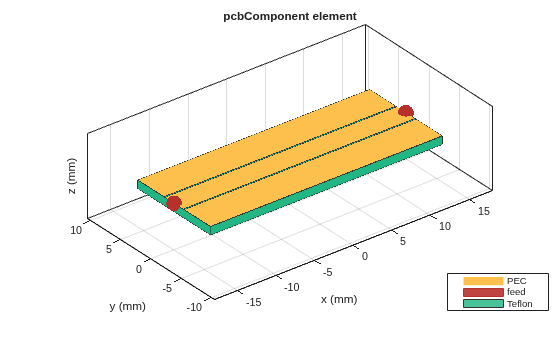
    Figure contains an axes object. The axes object with title pcbComponent element, xlabel x (mm), ylabel y (mm) contains 5 objects of type patch, surface. These objects represent PEC, feed, Teflon.

    Compute and plot S-parameters for the waveguide.

    s = sparameters(p, linspace(1e9, 5e9, 51));
    figure; rfplot(s)
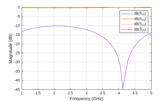
    Figure contains an axes object. The axes object with xlabel Frequency (GHz), ylabel Magnitude (dB) contains 4 objects of type line. These objects represent dB(S_{11}), dB(S_{21}), dB(S_{12}), dB(S_{22}).

    Version History

    Introduced in R2024b

    See Also

    Objects

    Topics