PCB Feeds
This topic discusses RF feed basics applying to RF PCBs and the specific ways to set up feeds in a PCB component.
Basic Feed Concepts
Feeds provide signal input and output interfaces to printed circuit boards (PCB). Feed ports on the PCB may be placed along a board edge, or within the interior of the board (away from any edge). Feeds can be implemented on single layer and multi-layer PCBs. From the feed port the signal will be routed internally within a PCB layer. In a multi-layer board the signal may also be routed between various layers through conductive vias.
There are two fundamental types of signal feeds, whether serving as an input or output port:
Single-ended (also called unbalanced) feed.
A single-ended feed consists of one signal line and a ground return. In a single-ended configuration the signal is measured between the signal trace and the ground return. The most common type of single-ended PCB feed is a microstrip line, that consists of a signal trace, usually on the top board layer, and a ground plane on a layer directly below the top layer.
This figure shows a microstrip transmission line created using the
microstripLineobject. Two red balls indicate signal ports locations. Note that the red balls do not represent any kind of physical connection or connector, but only port locations. For information on physical feeds see User-Defined Feeds.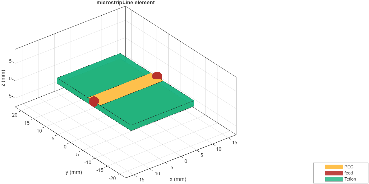
Differential (also called balanced) feed.
A differential feed consists of two coplaner signal lines. An optional ground plane is included to control impedance and provide shielding. The signal is measured across the two signal lines, that are 180 degrees out of phase. A common differential configuration feed implementation is an edge-coupled differential stripline where two parallel lines share identical electrical and physical characteristics.
Differential feeds provide excellent immunity to external ingress of electromagnetic signals, including noise, because coupled external signals result in a common mode signal across the pair of lines that cancel out when measured across the pair. Differential feeds reduce unintentional radiation of internally generated signals because the external electromagnetic fields from the pair of lines cancel each other, resulting in EMI reduction, and improved signal integrity within the PCB.
The figure shows a balanced transmission line created using the
coupledStripLineobject. Four red hemispheres indicate signal port locations. Note that the red hemispheres do not represent any kind of physical connection or connector, but only port locations. For information on physical feeds see User-Defined Feeds.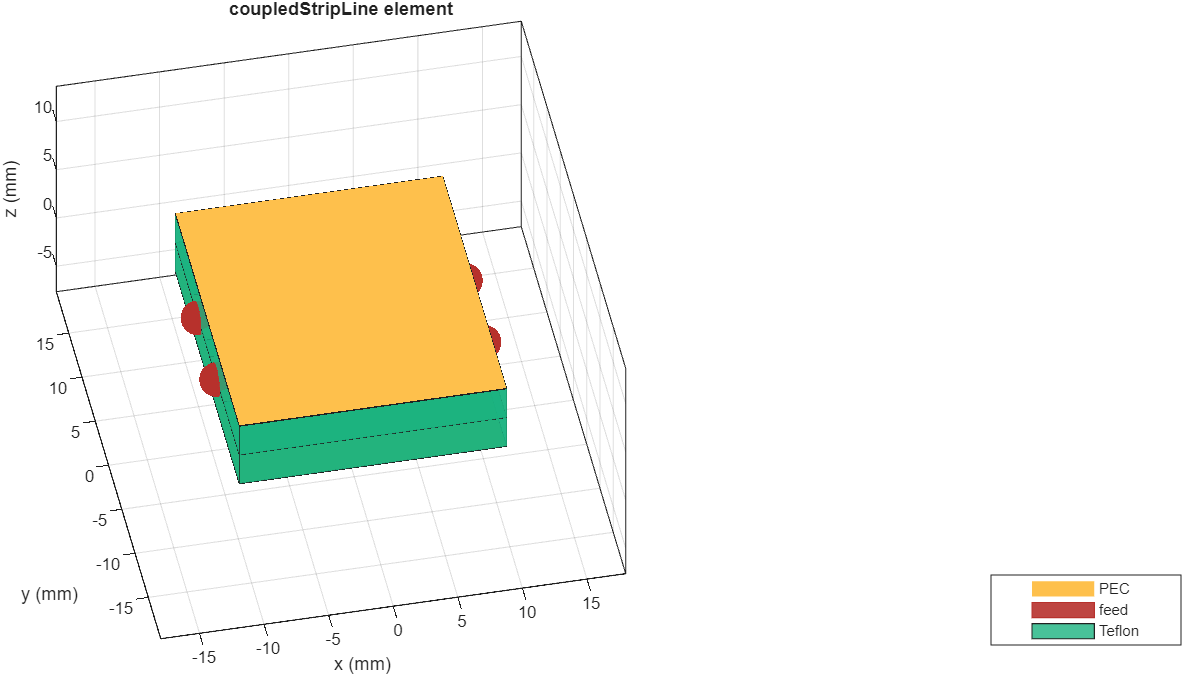
Feed Formats in RF PCB Toolbox
The way RF PCB Toolbox handles feeds is determined by setting FeedFormat
property in pcbComponent
object by locations as FeedLocations, or by feed type as
FeedDefinitions. This process starts by creating an object from the
PCB Components Catalog and converting it
to a pcbComponent
object. A pcbComponent can also be directly created from scratch.
Location-Defined Feeds
When starting with a PCB object created from the PCB Components Catalog, feed locations
are determined as part of object creation. When this object is converted to a
pcbComponent properties of the original object, including feed
locations are retained.
When creating a pcbComponent from scratch the feed locations must be
specified using FeedLocations
property.
By default, feed format in a pcbComponent is
set to FeedLocations. In this case the type of feed at feed locations is
automatically set up by the software based on the type of object and its geometry. The feed
details are not revealed, and cannot be changed. The advantage of using location-based feeds
is that you do not have to select the appropriate feed type, and manually create feed
geometry. When using location-defined feeds, any analysis of a PCB element, such as s
parameters, employ the automatically created feed. Ensure FeedFormat
property is set to "FeedLocations" in the pcbComponent
object.
Note
When starting with a PCB Components Catalog object you must
first convert the object to a PCB component object by entering pcb =
pcbComponent(catalogcomponent) in the command line, where
"catalogcomponent" in the name of the catalog object.
User-Defined Feeds
The other way to work with feeds is to manually create feeds using available feed
definition objects supported in the pcbComponent
object .The advantage of this method is that you can manually select the feed type and
control its detailed geometry. Experience with RF PCB feed applications and geometry is
recommended to efficiently use this method. As with location-defined feeds, the starting
point for user-defined feeds is a PCB Components Catalog object, converted to a
pcbComponent, or creating a pcbComponent from
scratch including specifying the feed locations.
To create user-defined feeds:
FeedFormat property must be set to
"FeedDefinition"in thepcbComponentobject.Use FeedDefinitions property to set feed type in the
pcbComponentobject. There is a choice of six feed types that can be configured. The choice of which feed type to use depends on the application of the PCB element.Configure chosen feed type from within individual feed-type object.
For further details on creating and configuring user-defined RF PCB feeds refer to individual feed-type reference pages.
This table shows typical applications for feed definitions supported in pcbComponent.
Feed-type Applications
| Type | Applications |
ProbeFeed | Microstrip patch antennas; vertical launch feed |
EdgeFeed | Microstrip elements whose signal originates on the PCB edge with one plane; stripline elements with two ground planes |
DeltaGapFeed | Balanced structures, dipole antennas, lumped loads |
CoaxialFeed | Higher-resolution version of a probe feed |
FiniteGapFeed | Coplanar multi-ground edge feeds, finite-width delta-gap feed |
ArbitraryFiniteGapFeed | Complex feed in which one or more signal locations are excited with respect to one or more ground locations |
Probe Feed
The ProbeFeed is a
type of contact feed used for patch antennas, or where a vertical PCB feed configuration
is required. Feed point is placed anywhere in the antenna element, which facilitates
impedance matching. Figures show probe placement, and feed properties.
Edge Feed
The EdgeFeed is a
type of contact feed used when an edge connection to a PCB element is required. An edge
feed is used with either microstrip elements, or stripline elements with two
grounds.
The figure shows an exploded view of an edge feed to a stripline element with two grounds. Captions in the figure correspond to feed Properties you can specify.
Delta Gap Feed
The DeltaGapFeed is
a type of contact feed used for balanced structures, dipole antennas and lumped
loads.
Captions in the figure show Properties you can set.
Coaxial Feed
The CoaxialFeed is a
type of direct contact feed. It is similar to the probe feed, but provides higher
resolution. The figure shows an exploded view of a coaxial feed. Signal is fed to the
element layer using a via, which runs from the center conductor of a coaxial cable to the
via's pad. The via's antipad isolates the signal from ground. Coaxial ground runs to the
ground layer. Captions in the figure correspond to feed Properties you
can set.
The figure provides a detailed coaxial feed view.
Finite Gap Feed
The FiniteGapFeed is
a type of contact feed used for coplanar feed applications. The figure shows a single-gap
configuration. The captions correspond to Properties you
can set.
Arbitrary Finite Gap Feed
The ArbitraryFiniteGapFeed is a type of contact feed used for complex
configurations that include multiple signals and multiple grounds. The figure shows an
exploded view of an arbitrary finite gap feed. The captions correspond to Properties you can
set.
See Also
pcbComponent | ArbitraryFiniteGapFeed | FiniteGapFeed | CoaxialFeed | EdgeFeed | ProbeFeed | DeltaGapFeed