IO Pin
Libraries:
SoC Blockset /
Hardware Logic I/O
Description
The IO Pin block connects model signals to physical input and output (I/O) pins on the hardware board. It provides an interface between the design under test (DUT) in the FPGA reference model and the I/O pins on the hardware board. Use this block to integrate your DUT with the external peripheral chips through FPGA I/O pins.
Limitations
Use this block only when targeting AMD® devices.
Ports
Input
Input ports that connect the FPGA model to the output pins on the hardware board.
Use these ports to send signals from the FPGA model to the external pins. The block
creates an input port for each pin specified in the I/O Pins
table, with the Direction column set to Output
and the Name column specifying the pin name.
Data Types: Boolean
Output
Output ports that connect the FPGA model to the input pins on the hardware board.
Use these ports to receive signals from the external pins and send them to the FPGA
model. The block creates an output port for each pin specified in the I/O
Pins table, with the Direction column set to
Input and the Name column specifying the pin
name.
Data Types: Boolean
Parameters
To edit block parameters interactively, use the Property Inspector. From the Simulink® Toolstrip, on the Simulation tab, in the Prepare gallery, select Property Inspector.
Option to enable the pass-through simulation mode, specified as one of these options:
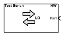
off— In this mode, the block acts as the I/O pins on the hardware board. Connect the input and output ports of the block to the FPGA model so that the model can read from and write to the external pins.on— In this mode, the block acts as a pass-through entity. The block labels its input and output ports on the mask as Test Bench and HW. Use these ports to pass input and output signals between the testbench and the FPGA model. Connect the ports on the Test Bench side to the testbench. Connect the ports on the HW side to the FPGA model.
List of I/O pins on the hardware board. Specify a string in Filter table contents to filter the list of available pins.
Name — Name of the I/O pin, specified as a string.
Direction — Direction of the I/O pin, specified as one of these options:
Output(default) — Set the pin direction toOutputwhen the FPGA model writes to the external pin. Use this pin to send a signal from the FPGA model to the output pin on the hardware board. The block adds this pin as an input port. In pass-through simulation mode, the block adds this pin as an input port on the HW side and as an output port on the Test Bench side.Input— Set the pin direction toInputwhen the FPGA model reads from the external pin. Use this pin to receive a signal from the input pin on the hardware board and send it to the FPGA model. The block adds this pin as an output port. In pass-through simulation mode, the block adds this pin as an output port on the HW side and as an input port on the Test Bench side.
Data Type — Data type of the I/O pin, specified as the
boolean.Pin — I/O pin number, specified as a string. The I/O pin number is different for each hardware board. To learn more about the pin numbers, see the board documentation.
IO Standard — I/O standard of the I/O pin, determined by the FPGA device and the specific I/O bank the pin belongs to. To learn more about the I/O standard of an I/O pin, see the board documentation.
Add a new pin by clicking New. Change the position of the selected pin by clicking Move Up or Move Down. Delete the selected pin by clicking Delete.
Extended Capabilities
To automatically generate HDL code for your design and execute the design on an SoC device, use one of these tools:
SoC Builder tool — For a tutorial using this tool, see Use SoC Builder to Generate SoC Design.
IP core generation workflow of the HDL Workflow Advisor tool — For an example using this workflow, see Use IP Core Generation Workflow with SoC Models.
Fixed-Point Conversion
Design and simulate fixed-point systems using Fixed-Point Designer™.
Version History
Introduced in R2026a
See Also
DIP Switch | LED | Push Button
MATLAB Command
You clicked a link that corresponds to this MATLAB command:
Run the command by entering it in the MATLAB Command Window. Web browsers do not support MATLAB commands.
Web サイトの選択
Web サイトを選択すると、翻訳されたコンテンツにアクセスし、地域のイベントやサービスを確認できます。現在の位置情報に基づき、次のサイトの選択を推奨します:
また、以下のリストから Web サイトを選択することもできます。
最適なサイトパフォーマンスの取得方法
中国のサイト (中国語または英語) を選択することで、最適なサイトパフォーマンスが得られます。その他の国の MathWorks のサイトは、お客様の地域からのアクセスが最適化されていません。
南北アメリカ
- América Latina (Español)
- Canada (English)
- United States (English)
ヨーロッパ
- Belgium (English)
- Denmark (English)
- Deutschland (Deutsch)
- España (Español)
- Finland (English)
- France (Français)
- Ireland (English)
- Italia (Italiano)
- Luxembourg (English)
- Netherlands (English)
- Norway (English)
- Österreich (Deutsch)
- Portugal (English)
- Sweden (English)
- Switzerland
- United Kingdom (English)