Support for I2C Communication
I2C, also known as Inter-Integrated Circuit, is a synchronous, chip-to-chip protocol for communication in integrated circuits and low speed peripherals. Some of the common I2C based devices include EEPROM, thermal sensors, and real-time clocks. The Simulink® Support Package for Arduino® Hardware library includes I2C Write block and I2C Read block that enable communication with I2C devices.
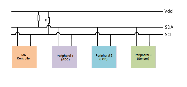
The I2C bus on the device has an I2C controller that is connected to two bidirectional lines, Serial Data Line (SDA) and Serial Clock Line (SCL). These two lines are connected to a pair of pins on the attached I2C peripheral device. The I2C peripheral device has a unique 7-bit or 10-bit address that is usually provided by the manufacturer. If the address is not unique, refer to the device data sheet to reconfigure the address.
The controller node generates a clock and initiates a communication with the peripheral device. The peripheral node receives the clock and responds with an acknowledgment to the I2C controller.
I2C uses the following communication modes:
Controller Transmit: I2C controller WRITES data to I2C peripheral
Controller Receive: I2C controller READS data from I2c peripheral
Peripheral Transmit: I2C peripheral WRITES data to I2C controller
Peripheral Receive: I2C peripheral READS data from I2C controller

Start and Stop Conditions
An I2C message consists of a START bit, the data to transmitted and a STOP bit.
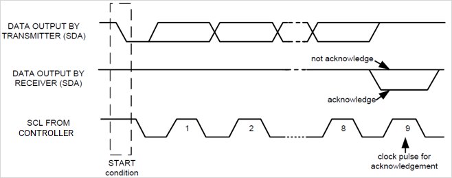
An SDA going from HIGH to LOW with the SCL still at HIGH indicates a START condition. The SDA going from LOW to HIGH with the SCL held at HIGH indicates a STOP condition. All other SDA transitions take place with SCL at low.

Data Acknowledgment
I2C communication defines the data bytes to be 8-bit long. I2C can transmit data of single byte or multiple bytes. During the data transmission, an acknowledge ACK signal follows every byte. A clock for ACK is generated by the controller, while the receiver (controller or peripheral) generates the ACK by pulling down the SDA and holding it to LOW during the high portion of the acknowledge clock pulse.
If the SDA is not pulled LOW during the acknowledge period, it indicates NACK (Not Acknowledge) by the receiver. If peripheral is not ready for transmit or receive of next data byte, it holds SCL LOW making the controller enter a WAIT state. Once the peripheral is ready and releases the SCL, the normal data transfer resumes.

I2C Read/Write
The I2C read/write operation takes place as follows:
The I2C controller initiates the communication by sending a START condition followed by a 7-bit peripheral address and the 8th bit to indicate write (0)/ read (1)).
The controller releases the SDA and waits for an ACK from the peripheral device.
If the peripheral exists on the bus, it responds with an ACK.
The controller continues in either transmit or receive mode (according to the read or write bit it sent), and the peripheral continues in its complementary mode (receive or transmit, respectively).
The controller terminates the data transmission by sending a STOP condition.
The following image shows a single byte read and write on an I2C peripheral device.


I2C Register Read/Write
The I2C register read/write operation takes place as follows:
The I2C controller initiates the communication by sending a START condition followed by a 7-bit peripheral address and the 8th bit to indicate write (0)/ read (1).
The controller releases the SDA and waits for an ACK from peripheral device.
If the peripheral exists on the bus, it responds with an ACK.
Then, the controller writes the register address of the peripheral it wants to access.
Once the peripheral acknowledges the register address, the controller sends the data byte with an ACK after each byte for write/read.
The controller terminates the data transmission by sending a STOP condition.
The following image shows a single byte read and write on a register present in the I2C peripheral device.

