GDDR5 x32 Implementation Kit
Implement a 32-bit GDDR5 interface for pre-layout analysis or post-layout verification.
GDDR5 (double data rate type five) SGRAM (synchronous graphics random access memory) is a high bandwidth interface designed for use in graphics cards, game consoles and high-performance computing. GDDR5 interfaces are capable of speeds of 7 Gb/s, with the goal of reaching 8 Gb/s.
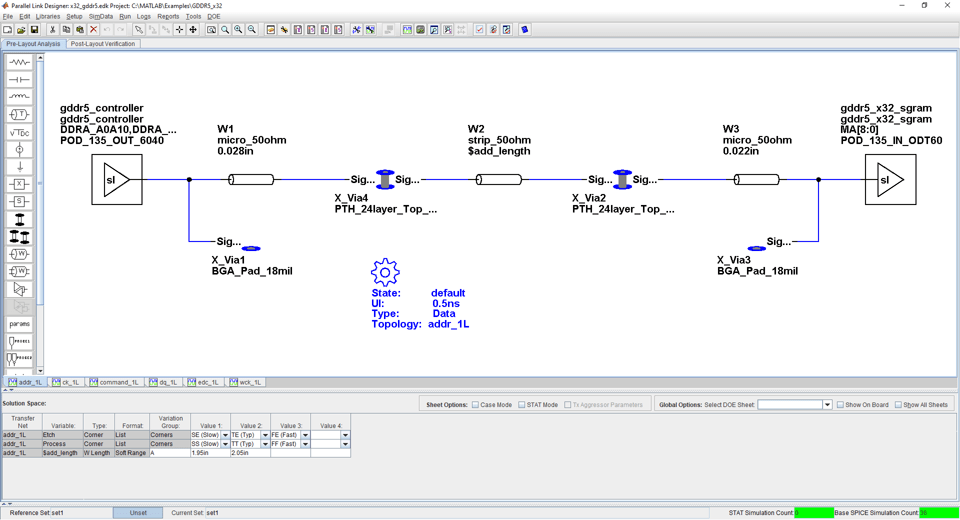
This GDDR5 implementation signal integrity kit includes all the transfer nets, timing models, waveform processing levels and simulation models for a GDDR5 x32 memory down interface. This includes buffer models for a generic GDDR5 controller and Micron x32 8 Gb SGRAM, along with timing models and complete waveform processing levels.
You can modify the kit to match your exact DDR5 implementation. Then, perform complete pre-layout solution space analysis and/or full post-layout verification for waveform quality and timing margins.
Open GDDR5 x32 Kit
Open the GDDR5 x32 kit in the Parallel Link Designer app using the openSignalIntegrityKit function.
openSignalIntegrityKit("GDDR5_x32");
Kit Overview
Project name: GDDR5_x32
Interface name: x32_gddr5
Target data rate: 4 Gb/s (UI = 250 ps)
This kit supports both HSPICE and IsSpice4 simulators. No specific version of either simulator is required when running this kit.
For more information about the generic GDDR5 x32 implementation signal integrity kit, including block diagrams, system configurations, transfer nets and libraries, refer to the document GDDR5_x32.pdf located inside the kit project directory.
References
[1] JEDEC: Graphics Double Data Rate (GDDR5) SGRAM Standard. JESD212B.01. December 2013.
[2] JEDEC: POD135 – 1.35V Pseudo Open Drain I/O. JESD8-21A. September 2013.
[3] Micron: GDDR5 SGRAM for Networking – MT51K256M32 – 16Meg x32 I/O x16 Banks, 32Meg x16 I/O x16 Banks. Rev. A 5/14 EN.
[4] Micron: Technical Note: GDDR5 SGRAM Introduction. Rev. A 2/14 EN.