Static Var Compensator (Phasor Type)
Implement phasor model of three-phase static var compensator
Description
The Static Var Compensator (SVC) is a shunt device of the Flexible AC Transmission Systems (FACTS) family using power electronics to control power flow and improve transient stability on power grids [1]. The SVC regulates voltage at its terminals by controlling the amount of reactive power injected into or absorbed from the power system. When system voltage is low, the SVC generates reactive power (SVC capacitive). When system voltage is high, it absorbs reactive power (SVC inductive). The variation of reactive power is performed by switching three-phase capacitor banks and inductor banks connected on the secondary side of a coupling transformer. Each capacitor bank is switched on and off by three thyristor switches (Thyristor Switched Capacitor or TSC). Reactors are either switched on-off (Thyristor Switched Reactor or TSR) or phase-controlled (Thyristor Controlled Reactor or TCR).
The figure below shows a single-line diagram of a static var compensator and a simplified block diagram of its control system.
Single-line Diagram of an SVC and Its Control System Block Diagram
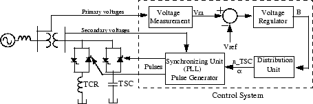
The control system consists of
A measurement system measuring the positive-sequence voltage to be controlled. A Fourier-based measurement system using a one-cycle running average is used.
A voltage regulator that uses the voltage error (difference between the measured voltage Vm and the reference voltage Vref) to determine the SVC susceptance B needed to keep the system voltage constant
A distribution unit that determines the TSCs (and eventually TSRs) that must be switched in and out, and computes the firing angle α of TCRs
A synchronizing system using a phase-locked loop (PLL) synchronized on the secondary voltages and a pulse generator that send appropriate pulses to the thyristors
The SVC (Phasor Type) block is a phasor model, and you must use it with the phasor simulation method, activated with the Powergui block. It can be used in three-phase power systems together with synchronous generators, motors, and dynamic loads to perform transient stability studies and observe impact of the SVC on electromechanical oscillations and transmission capacity. This model does not include detailed representations of the power electronics, the measurement system, or the synchronization system. These systems are approximated rather by simple transfer functions that yield a correct representation at the system's fundamental frequency.
A detailed model of a SVC using three TSCs and one TCR is provided in the
power_svc_1tcr3tsc example.
SVC V-I Characteristic
The SVC can be operated in two different modes:
In voltage regulation mode (the voltage is regulated within limits as explained below)
In var control mode (the SVC susceptance is kept constant)
When the SVC is operated in voltage regulation mode, it implements the following V-I characteristic.
SVC V-I characteristic
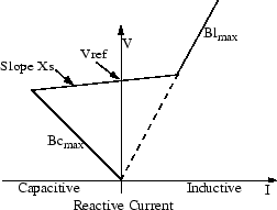
As long as the SVC susceptance B stays within the maximum and minimum susceptance values imposed by the total reactive power of capacitor banks (Bcmax) and reactor banks (Blmax), the voltage is regulated at the reference voltage Vref. However, a voltage droop is normally used (usually between 1% and 4% at maximum reactive power output), and the V-I characteristic has the slope indicated in the figure. The V-I characteristic is described by the following three equations:
where
V | Positive sequence voltage (pu) |
I | Reactive current (pu/Pbase) (I > 0 indicates an inductive current) |
Xs | Slope or droop reactance (pu/Pbase) |
Bcmax | Maximum capacitive susceptance (pu/Pbase) with all TSCs in service, no TSR or TCR |
Blmax | Maximum inductive susceptance (pu/Pbase) with all TSRs in service or TCRs at full conduction, no TSC |
Pbase | Three-phase base power specified in the block dialog box |
SVC Dynamic Response
When the SVC is operating in voltage regulation mode, its response speed to a change of system voltage depends on the voltage regulator gains (proportional gain Kp and integral gain Ki), the droop reactance Xs, and the system strength (short-circuit level).
For an integral-type voltage regulator (Kp = 0), if the voltage measurement time constant Tm and the average time delay Td due to valve firing are neglected, the closed-loop system consisting of the SVC and the power system can be approximated by a first-order system having the following closed-loop time constant:
Tc = 1 / (Ki(Xs + Xn))
where
Tc | Closed loop time constant |
Ki | Proportional gain of the voltage regulator (pu_B/pu_V/s) |
Xs | Slope reactance pu/Pbase |
Xn | Equivalent power system reactance (pu/Pbase) |
This equation demonstrates that you obtain a faster response speed when the regulator gain is increased or when the system short-circuit level decreases (higher Xn values). If you take into account the time delays due to voltage measurement system and valve firing, you obtain an oscillatory response and, eventually, an instability with too weak a system or too large a regulator gain.
Parameters
The SVC parameters are grouped in two categories: Power Data and
Control Parameters. Use the Display listbox
to select which group of parameters you want to visualize.
Power Tab
- Ignore negative-sequence current
The SVC is modeled by a three-wire system using two current sources. The SVC does not generate any zero-sequence current, but it can generate negative-sequence currents during unbalanced system operation. The negative-sequence susceptance of the SVC is assumed to be identical to its positive-sequence value, as determined by the B value computed by the voltage regulator.
Select this box to ignore negative-sequence current. Default is selected.
- Nominal voltage and frequency
The nominal line-to-line voltage in Vrms and the nominal system frequency in hertz. Default is
[500e3, 60].- Three-phase base power
Three-phase base power, in VA, used to specify the following parameters in pu: droop reactance Xs, gains Kp and Ki of the voltage PI regulator, and reference susceptance Bref. This base power is also used to normalize the output B susceptance signal. Default is
200e6.- Reactive power limits
The maximum SVC reactive powers at 1 pu voltage, in vars. Enter a positive value for the capacitive reactive power Qc (vars generated by the SVC) and a negative value for the inductive reactive power Ql (vars absorbed by the SVC). Default is
[200e6, -200e6].- Average time delay due to thyristor valves firing
Average time delay simulating the non instantaneous variation of thyristor fundamental current when the distribution unit sends a switching order to the pulse generator. Because pulses have to be synchronized with thyristor commutation voltages, this delay normally varies between 0 and 1/2 cycle. The suggested average value is 4 ms. Default is
4e-3.
Controller Tab
- Mode
Specifies the SVC mode of operation. Select either
Voltage
         regulation
(default) orVar control (Fixed susceptance Bref).- Reference voltage Vref
This parameter is not available when the Mode parameter is set to
Var control (Fixed susceptance Bref)or when External is selected.Reference voltage, in pu, used by the voltage regulator. Default is
1.0.- External
When External is selected, a Simulink® input named Vref appears on the block, allowing you to control the reference voltage from an external signal (in pu). The Reference voltage parameter is therefore unavailable. Default is selected.
- Droop Xs
This parameter is not available when the Mode parameter is set to
Var control (Fixed susceptance Bref).Droop reactance, in pu/Pbase, defining the slope of the V-I characteristic. Default is
0.03.- Voltage regulator gains
This parameter is not available when the Mode parameter is set to
Var control (Fixed susceptance Bref).Proportional gain, in (pu of B)/(pu of V), and integral gain, in pu_B/pu_V/s, of the voltage regulator. Default is
[0 300].- Susceptance Bref
This parameter is not available when the Mode parameter is set to
Voltage regulation.Reference susceptance, in pu/Pbase, when the SVC is operating in var control mode. Default is
0.0.
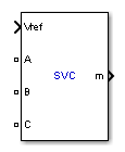
Inputs and Outputs
A B CThe three terminals of the SVC.
VrefSimulink input of the reference voltage signal.
This input is visible only when the External control of reference voltage Vref parameter is checked.
mSimulink output vector containing six SVC internal signals. These signals are either voltage and current phasors (complex signals) or control signals. They can be individually accessed by using the Bus Selector block. They are, in order:
Signal
Signal Group
Signal Names
Definition
1-3
Power Iabc (cmplx)
Ia(pu) Ib(pu)
Ic(pu)Phasor currents Ia, Ib, Ic flowing into the SVC (pu)
4
Control
Vm (pu)
Positive-sequence value of measured voltage (pu)
5
Control
B (pu)
SVC susceptance output of the voltage regulator (pu). A positive value indicates that the SVC is capacitive.
6
Control
Q (pu)
SVC reactive power output (pu). A positive value indicates inductive operation.
Examples
The power_svc example
illustrate a static var compensator (SVC) used to regulate voltage on a 500 kV, 3000 MVA system.
When the system voltage is low, the SVC generates reactive power (SVC capacitive) and when the
system voltage is high it absorbs reactive power (SVC inductive).
References
[1] N. G. Hingorani, L. Gyugyi, “Understanding FACTS; Concepts and Technology of Flexible AC Transmission Systems,” IEEE® Press book, 2000
Version History
Introduced in R2006a
You can also select a web site from the following list:
Americas
- América Latina (Español)
- Canada (English)
- United States (English)
Europe
- Belgium (English)
- Denmark (English)
- Deutschland (Deutsch)
- España (Español)
- Finland (English)
- France (Français)
- Ireland (English)
- Italia (Italiano)
- Luxembourg (English)
- Netherlands (English)
- Norway (English)
- Österreich (Deutsch)
- Portugal (English)
- Sweden (English)
- Switzerland
- United Kingdom (English)