Model Electrical-Optical-Electrical Link for End-to-End IBIS-AMI Co-Simulation
R2026bThis example shows how to model a silicon photonic electrical-optical-electrical (EOE) link at 112 Gbps PAM4 using SerDes Toolbox. The optical domain is modeled with custom System objects that plug into the standard SerDes simulation framework, enabling end-to-end IBIS-AMI co-simulation of the electrical and optical channels.
Linear Pluggable Optics and System-Level Modeling
The optical interconnect landscape is shifting toward linear-drive pluggable optics (LPO). Unlike traditional pluggable modules that embed a retimer with full CDR and equalization inside the optical module, LPO removes the retimer and treats the optical path as a transparent analog channel. Related form factors include co-packaged optics (CPO), where the optical engine sits on the ASIC package, and near-package optics (NPO), where the module is adjacent to the ASIC but still separate.
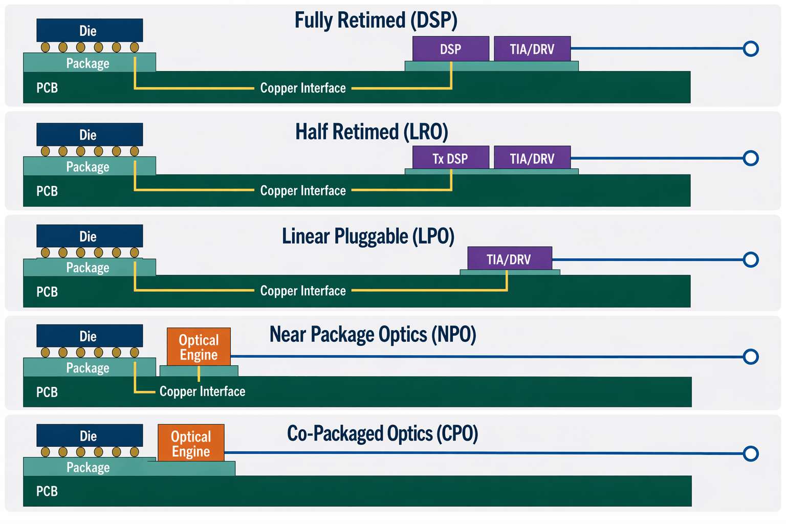
The key distinction for system modeling is:
With a retimer (traditional pluggable): the optical link is isolated. The host SerDes sees only the electrical channel to/from the module. No optical impairments leak through.
Without a retimer (LPO/CPO): the optical path impairments (modulator nonlinearity, bandwidth limitations, thermal drift) are directly visible to the host Rx equalizer. The entire electrical-optical-electrical path must be modeled as one channel.
This removal of the retimer is what motivates a end to end system-level simulation because the Tx/Rx SerDes must now equalize a signal considering both the electrical channels and the optical domain impairments. Standard SerDes/Signal Integrity concepts like channel analysis, eye diagram metrics, and equalization design strategies all still apply but the channel now includes active components with unfamiliar impairments such as ring modulator nonlinearity, photon lifetime bandwidth, and thermo-optic feedback.
The EOE Signal Chain
An EOE system replaces a section of the electrical channel with an optical hop. Inside this system, the signal passes through the below elements:
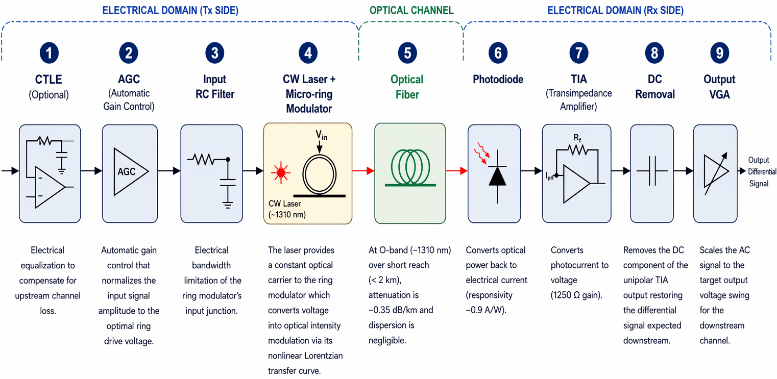
After the EOE system, the signal passes through a second analog channel and into the Rx equalizer.
The Micro-Ring Modulator
The ring modulator is the core electro-optic component and the primary source of optical-domain impairments. In through-port (all-pass) configuration, the ring creates a narrow notch in the transmission spectrum. The notch position shifts with applied voltage, and the optical carrier sits on the slope of this notch so that voltage changes translate to intensity changes.
Let's visualize the cold ring spectrum (no thermal shift) to see how voltage moves the notch. Each curve shows the optical transmission vs. wavelength at a different bias voltage:
ring = RingModulator;  % Defaults match the Simulink model configuration
wavelengths = linspace(1312.4, 1313.6, 500);
voltages = [-0.3, -0.1, 0, 0.1, 0.3];
figure
hold on
for v = voltages
    T = ring.getStaticTransmission(v, wavelengths);
    plot(wavelengths, 10*log10(T), 'DisplayName', sprintf('V = %.2f V', v))
end
xline(1313.0, 'r-', 'Laser', 'LineWidth', 2, 'LabelVerticalAlignment','bottom', 'DisplayName','Laser \lambda')
hold off
xlabel('Wavelength (nm)')
ylabel('Transmission (dB)')
title('Ring Spectrum at Cold Start (\DeltaT_{ring} = 0)')
legend('Location','east')
grid on
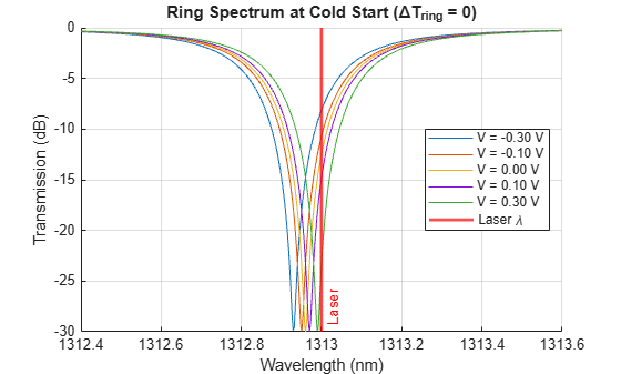
At the bottom of each notch (~-30 dB), transmission is only 0.1%; nearly all the laser power is absorbed inside the ring cavity as heat. This is a single-bus all-pass ring: one waveguide transfers energy to the ring via evanescent coupling across a narrow gap, with no drop port, so all input light either passes through or is absorbed. Energy conservation requires that the non-transmitted fraction equals the absorbed power, and this drives the thermal model.
Notice in the plot how the notch shifts right with increasing voltage; that voltage-to-position shift is what encodes the electrical signal onto the light. On this cold ring, the laser sits near the notch bottom for positive voltages. In operation, thermal self-heating shifts the resonance away from the laser, placing the laser on the slope where modulation is effective.
Transfer Function and Block Parameters
The equation governing the ring is a Lorentzian (the optical equivalent of a single-pole resonance):
where the detuning is the difference between the laser wavelength and the ring's current resonance:
The resonance wavelength shifts with both voltage and temperature rise (throughout this model, temperature is expressed as degrees above ambient: a , not absolute temperature):
Each variable maps directly to a block mask parameter in the Simulink model:
= 1313.0 nm: LaserSource block,
CentralWavelength. The continuous wave (CW) laser emission wavelength.= 1312.96 nm: RingModulator block,
ResonanceWavelength. Ring resonance at zero volts and zero temperature rise.= 4000: RingModulator block,
Q. Quality factor controlling notch sharpness.= 0.999: RingModulator block,
Amin. Extinction at resonance (~30 dB depth).= 0.10 nm/V: RingModulator block,
TuningCoefficient. Electro-optic tuning rate (representative of enhanced depletion or MOSCAP designs).= 0.07 nm/K: RingModulator block,
ThermalCoefficient. Thermo-optic drift rate.1.98 K: ThermalNetwork block output. Ring temperature rise above ambient at steady state.
The following annotated plot shows how these parameters map to the cold notch shape (V=0, no thermal shift). The FWHM (full width at half maximum, equal to ) sets the scale for everything: the detuning and voltage-induced shifts are meaningful relative to the FWHM. A shift of 0.1 nm matters a lot when FWHM is 0.33 nm, but would be negligible on a broader notch.
lambdaPlot = linspace(1312.4, 1313.6, 1000);
T_plot = ring.getStaticTransmission(0, lambdaPlot);
T_dB = 10*log10(T_plot);
FWHM = ring.ResonanceWavelength / ring.Q;
resWL = ring.ResonanceWavelength;
figure
plot(lambdaPlot, T_dB, 'b', 'LineWidth', 1.5)
hold on
% Mark resonance wavelength
xline(resWL, '--', '\lambda_{res,0}', 'LineWidth', 1.5, 'Color', [1 0.6 0], 'LabelVerticalAlignment', 'bottom', 'LabelHorizontalAlignment', 'left')
% Mark laser wavelength
xline(1313.0, 'r-', '\lambda_{laser}', 'LineWidth', 2, 'LabelVerticalAlignment', 'bottom', 'LabelHorizontalAlignment', 'right')
% Annotate FWHM
halfMax_dB = 10*log10(1 - ring.Amin/2);  % -3 dB point of Lorentzian
yline(halfMax_dB, ':', 'Color', [0.5 0.5 0.5])
plot(resWL + [-1 1]*FWHM/2, [halfMax_dB halfMax_dB], 'm-', 'LineWidth', 2)
text(resWL, halfMax_dB - 2, sprintf('FWHM = \\lambda/Q = %.2f nm', FWHM), ...
    'HorizontalAlignment', 'center', 'Color', 'm', 'FontWeight', 'bold')
% Annotate Amin (extinction depth)
plot(resWL, 10*log10(1-ring.Amin), 'v', 'MarkerSize', 10, 'MarkerFaceColor', [0.85 0.33 0.1], 'Color', [0.85 0.33 0.1])
text(resWL + 0.05, 10*log10(1-ring.Amin) + 2, sprintf('A_{min} = %.3f (%.0f dB)', ring.Amin, 10*log10(1-ring.Amin)), ...
    'FontWeight', 'bold', 'Color', [0.85 0.33 0.1])
% Annotate detuning
detuning = 1313.0 - resWL;
plot([resWL, 1313.0], [-2 -2], 'g-', 'LineWidth', 2)
text(resWL + detuning/2, -0.5, sprintf('Detuning = %.2f nm', detuning), ...
    'HorizontalAlignment', 'center', 'Color', [0 0.6 0], 'FontWeight', 'bold')
hold off
xlabel('Wavelength (nm)')
ylabel('Transmission (dB)')
title('Ring Notch Anatomy: Key Parameters')
ylim([-35 2])
grid on
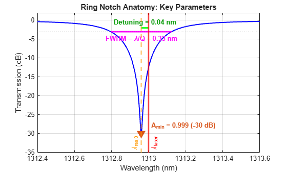
Here's how these parameters affect link performance:
Quality factor Q: controls notch sharpness. Higher Q = narrower notch = steeper slopes = more modulation efficiency per volt, but also narrower modulation bandwidth and higher sensitivity to drift. The photon lifetime (where is the resonance wavelength and is the speed of light) sets a fundamental speed limit: the 3 dB modulation bandwidth is . At Q=4000 this gives 57.1 GHz. In effect, the ring acts as a single-pole low-pass filter on the modulated signal; fast transitions are attenuated, creating ISI just as a bandwidth-limited electrical channel would. At Q=4000 the photon lifetime bandwidth (57.1 GHz) is above the photodiode and TIA bandwidths (50 GHz each), so those components currently dominate the bandwidth budget. However, increasing Q makes the photon lifetime the tightest pole: at Q=8000 it drops to 28.5 GHz, well below Nyquist for 56 GBaud. The Q-bandwidth tradeoff is analogous to the gain-bandwidth product of an amplifier.
: the extinction ratio at resonance. How deep the notch goes (0.999 means ~30 dB extinction).
Tuning coefficient : how much the notch shifts per volt of drive. This is the electro-optic modulation mechanism.
Thermal coefficient : how much the notch shifts per degree of temperature change. This creates a feedback loop described next.
Parameter dependencies: Not all parameters can be changed independently. If you change Q, you must also update Output_Optical_BW.PeakingFrequency (which equals ) and recalculate the self-consistent thermal operating point (InitialAbsorbedPower, DefaultTemperature, ResonanceWavelength). Changing TuningCoefficient affects the optimal AGC drive level. Changing ResonanceWavelength or LaserSource.CentralWavelength shifts the detuning and requires a new thermal equilibrium.
Thermo-Optic Feedback
When light passes through the ring, some optical power is absorbed and converted to heat. This temperature rise shifts the resonance wavelength (70 pm/K), which changes the transmission, which changes the absorbed power; creating a feedback loop. This is analogous to self-heating in a high-power driver shifting its bias point over time, except here the effect is on the optical transfer curve rather than the I-V characteristic.
This feedback can cause:
Slow drift of the operating point during a burst
Bistability where two stable operating temperatures exist for the same input
Pattern-dependent heating where the ring temperature depends on recent data history
The thermal model (ThermalNetwork) implements a discrete-time state-space model of 1D heat conduction from the ring waveguide (heat source, x=0) through the silicon substrate to a fixed-temperature heat sink (package thermal ground, x=L). It discretizes the conduction path into 40 spatial nodes and advances the temperature profile each sample using implicit finite-difference matrices. It outputs the ring temperature based on the previous time step's absorbed power, so the feedback loop updates naturally each sample without any special handling in the model.
The key ThermalNetwork mask parameter is InitialAbsorbedPower, which sets the starting temperature via the analytical steady-state solution. In this model it is set to 0.000739 W, giving an initial temperature rise of ~1.98 K. The steady-state ring temperature depends on the thermal resistance from the ring to the heat sink, set by the ThermalNetwork mask parameters L (path length), SourceRegionWidth, and ThermalConductivity.
With thermal shift included, the spectrum looks quite different from the cold ring shown earlier. The resonance moves to ~1313.10 nm, placing the laser on the left slope where all PAM4 drive levels produce well-separated transmission values:
figure
hold on
for v = [-0.3, -0.1, 0, 0.1, 0.3]
    T = ring.getStaticTransmission(v, wavelengths - ring.ThermalCoefficient * 1.98);
    plot(wavelengths, 10*log10(T), 'DisplayName', sprintf('V = %.2f V', v))
end
xline(1313.0, 'r-', 'Laser', 'LineWidth', 2, 'LabelVerticalAlignment','bottom', 'DisplayName','Laser \lambda')
hold off
xlabel('Wavelength (nm)')
ylabel('Transmission (dB)')
title('Ring Spectrum at Operating Point (\DeltaT_{ring} = +1.98 K)')
legend('Location','east')
grid on
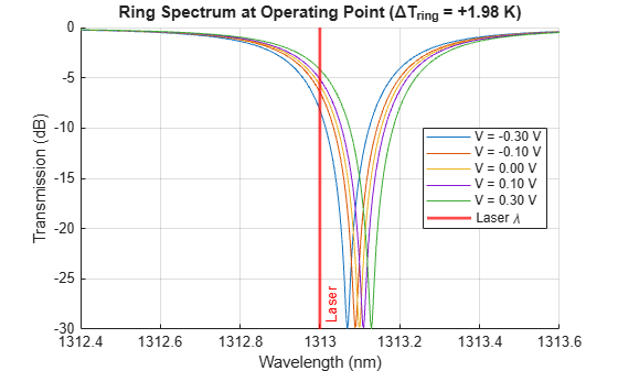
Compare this with the cold spectrum above: thermal self-heating has moved the notch to the right, and the laser now sits well up the left slope. The five voltage curves are clearly separated at the laser wavelength, confirming effective PAM4 modulation at this operating point. The plot shows five voltages: the four PAM4 levels (-0.3, -0.1, 0.1, 0.3 V) plus 0 V as a reference marking the midpoint of the drive swing.
Here's how the operating point numbers work out:
The laser emits at 1313.0 nm (
LaserSource.CentralWavelength)The ring's cold resonance is at 1312.96 nm (
RingModulator.ResonanceWavelength)At steady state the ring absorbs ~0.74 mW (
ThermalNetwork.InitialAbsorbedPower), heating it by ~1.98 KThat shifts the resonance by 0.07 nm/K 1.98 K = 0.139 nm
Effective resonance: 1312.96 + 0.139 = 1313.10 nm
The gap between laser (1313.0 nm) and effective resonance (1313.10 nm) is 0.10 nm. With Q=4000 the notch FWHM is only 0.33 nm, so this detuning places the laser about 0.3 FWHM from resonance; near the steepest part of the slope. The steeper the slope at the operating point, the more the transmission changes per volt of drive.
Let's see how different absorbed power levels shift the transfer curve via this thermal feedback. The middle curve (739 uW) is the nominal operating point:
laser = LaserSource;  % Defaults match Simulink model
laserWavelength = laser.CentralWavelength;
absorbedPowers = [0.0004, 0.000739, 0.0011];  % W
vSweep = linspace(-0.5, 0.5, 200);
tn = ThermalNetwork;
tn(0);  % First call initializes solver grid
figure
hold on
for pAbs = absorbedPowers
    profile = tn.computeSteadyStateProfile(pAbs);
    Tring = profile(1);  % Temperature at ring face
    % Shift laser wavelength to account for thermal resonance shift
    % (equivalent to setting InternalTemperature inside the ring)
    thermalShift = ring.ThermalCoefficient * Tring;
    effectiveLaser = laserWavelength - thermalShift;
    Tr = ring.getStaticTransmission(vSweep, effectiveLaser);
    effectiveRes = ring.ResonanceWavelength + thermalShift;
    plot(vSweep, Tr, 'LineWidth', 1.5, ...
        'DisplayName', sprintf('P_{abs} = %.0f \\muW (T = %.2f K, \\lambda_{res} = %.2f nm)', pAbs*1e6, Tring, effectiveRes))
end
hold off
xlabel('Input Voltage (V)')
ylabel('Optical Transmission')
title('Transfer Curve Shift Due to Thermal Feedback')
ylim([0 0.6])
legend('Location','best')
grid on
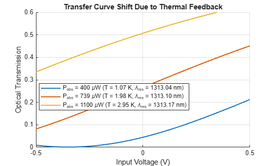
Higher absorbed power shifts the curve to the right (the resonance wavelength increases with temperature). Because the laser wavelength is fixed, this effectively moves the operating point leftward on the curve toward the steeper slope. This creates a stabilizing (negative) feedback loop: a burst of PAM4 symbol-0 (the lowest voltage level, which sits deepest in the notch and absorbs the most power) heats the ring, shifting the curve rightward and moving the operating point away from the notch bottom. This reduces absorption and counteracts the temperature rise. The system settles at the middle curve (739 uW), where absorbed power and thermal dissipation are in balance.
PAM4 Levels on the Transfer Curve
The transfer curve is inherently nonlinear; unlike an electrical VGA, the ring does not have a flat gain region. For PAM4 signaling, this nonlinearity creates unequal eye spacing (level compression), similar to what you'd see from a saturating driver.
A PAM4 signal has four voltage levels. With a typical swing of approximately 0.3 V around zero, the four levels map to different points on the nominal transfer curve (middle curve above):
thermalShift_op = ring.ThermalCoefficient * 1.98;
effectiveLaser_op = laserWavelength - thermalShift_op;
pam4Levels = [-0.3, -0.1, 0.1, 0.3]';  % Approximate PAM4 drive levels
T_levels = ring.getStaticTransmission(pam4Levels, effectiveLaser_op);
absorption = (1 - T_levels) * 100;
OMA = max(T_levels) - min(T_levels);
extinctionRatio_dB = -10*log10(min(T_levels)/max(T_levels));
pam4Table = table(pam4Levels, T_levels, absorption, ...
    'VariableNames', {'Voltage (V)', 'Transmission', 'Absorption (%)'})
pam4Table = 4×3 table
    Voltage (V)    Transmission    Absorption (%)
    ___________    ____________    ______________

       -0.3          0.14959           85.041
       -0.1          0.22645           77.355
        0.1          0.30521           69.479
        0.3          0.38103           61.897

	Get insights using Copilot
fprintf('Modulation depth (OMA): %.3f (%.1f dB extinction ratio)\n', OMA, extinctionRatio_dB)Modulation depth (OMA): 0.231 (4.1 dB extinction ratio)
Modulation depth (OMA) is the Optical Modulation Amplitude: the difference in transmission between the highest and lowest PAM4 levels. It represents the total optical swing available for signaling. A larger OMA means more signal margin at the receiver.
Extinction ratio is the ratio of maximum to minimum optical power in dB: . It captures how well the modulator distinguishes "on" from "off." Higher extinction ratio generally improves receiver sensitivity, but for a ring modulator, pushing deeper into the notch (higher ER) also increases nonlinear level compression in PAM4, making the inner eye openings smaller.
Receiver Front-End: Photodiode + TIA
The optical receiver converts light back to an electrical signal in two stages, much like an electrical Rx AFE:
Photodiode: produces a current proportional to incident optical power (responsivity = 0.9 A/W). Optional shot noise modeling is available. A single-pole bandwidth filter (50 GHz) models the RC-limited response.
Transimpedance amplifier (TIA): converts photocurrent to voltage with a gain of 1250 ohms. Also bandwidth-limited (50 GHz single-pole) with optional input-referred noise.
Together, the photodiode and TIA determine the receiver sensitivity and noise floor, just as the AFE does in an electrical SerDes link.
Let's trace the PAM4 optical power levels through the receiver to see what electrical voltages come out. The laser emits 3 dBm (2 mW), but 3 dB of optical path loss (coupling, routing) cuts that in half, delivering 0 dBm (1 mW) to the ring:
laserPower_W = 1e-3;  % 1 mW net at ring input (2 mW emitted, half lost to coupling)
opticalPower_W = laserPower_W * T_levels;  % After ring modulation
pd = Photodiode;    % Defaults: 0.9 A/W, 50 GHz BW
tia = TransimpedanceAmplifier;  % Defaults: 1250 ohms, 50 GHz BW
% Run each power level for enough samples to let bandwidth filters settle
nSettle = 200;
photocurrent_A = zeros(4,1);
voltage_V = zeros(4,1);
for k = 1:4
    reset(pd);
    reset(tia);
    for n = 1:nSettle
        I = pd(opticalPower_W(k));
        V = tia(I);
    end
    photocurrent_A(k) = I;
    voltage_V(k) = V;
end
rxTable = table(pam4Levels, T_levels, photocurrent_A*1e6, voltage_V*1e3, ...
    'VariableNames', {'Voltage (V)', 'Transmission', 'Photocurrent (uA)', 'TIA Output (mV)'})
rxTable = 4×4 table
    Voltage (V)    Transmission    Photocurrent (uA)    TIA Output (mV)
    ___________    ____________    _________________    _______________

       -0.3          0.14959            134.63              168.28
       -0.1          0.22645             203.8              254.75
        0.1          0.30521            274.69              343.37
        0.3          0.38103            342.92              428.65

	Get insights using Copilot
Simulink Model and Redriver Topology
In the IBIS framework, a redriver (Section 10, p. 295) is a repeater that sits between two channels and re-conditions the signal without recovering the clock. An EOE redriver occupies the same architectural slot as an electrical redriver: it sits between two analog channels (copper traces) and re-conditions the signal — but the internal signal path passes through the optical domain. This configuration is most analogous to near-package optics (NPO), where moderate-loss electrical traces connect the ASIC to a nearby optical module on either side.
model = 'eoeLink';
open_system(model);
The top-level model is:

The redriver is modeled as a back-to-back Rx/Tx pair:
The Rx subsystem receives the electrical signal from the upstream channel, processes it through the optical domain (modulator, fiber, photodiode, TIA), and outputs a re-conditioned electrical signal.
The Tx subsystem is a pass-through (no additional processing in this model).
The redriver framework allows you to split the datapath blocks across the Rx and Tx subsystems however you like. In this example we keep all processing in the Rx subsystem for simplicity. This Rx then Tx block ordering is standard for IBIS-AMI redriver models and handles the Init/GetWave processing.
The EOE redriver Rx subsystem signal chain implements the blocks described in the EOE Signal Chain section above:
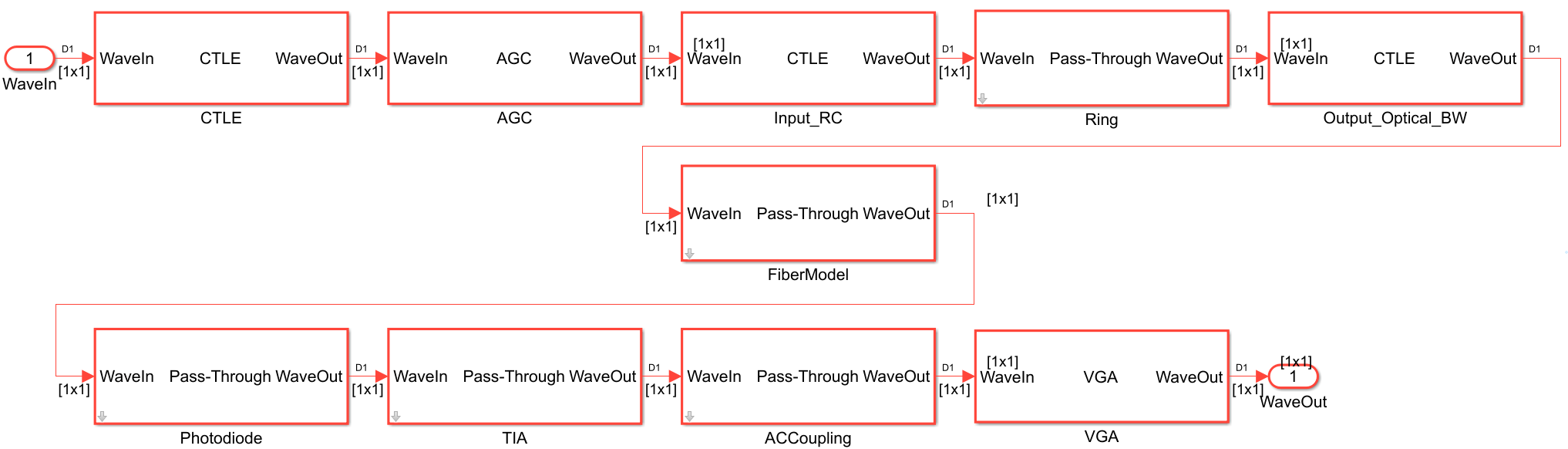
The blocks are a mix of SerDes Toolbox datapath blocks (CTLE, AGC, VGA) and custom optical matlab.System objects (RingModulator, LaserSource, LaserMixer, ThermalNetwork, OpticalFiber, Photodiode, TransimpedanceAmplifier). Two additional bandwidth filters — Input_RC and Output_Optical_BW — model the ring's input junction (100 GHz single-pole) and photon lifetime (57.1 GHz for Q=4000, from ). At higher Q values the photon lifetime becomes the dominant bandwidth constraint, limiting the ring's modulation speed and creating ISI that the downstream equalizer must compensate.
This model uses a single-wavelength, single-ring architecture: one high-speed ring modulator carrying PAM4 on a single optical carrier. An alternative approach used in some systems is wavelength-division multiplexing (WDM), where multiple lower-speed rings each modulate a different wavelength using simpler NRZ signaling, and a wavelength demux separates the channels at the receiver. The single-ring PAM4 approach modeled here trades WDM complexity for higher per-lane bandwidth and a simpler optical path (no demux needed).
One subtlety: IBIS-AMI signals are differential voltages centered at 0V, but optical power is inherently positive — you cannot have negative light. The ring modulator maps the differential input onto its Lorentzian transfer curve, creating a unipolar optical signal that swings around a DC operating point. The DC removal block (AC coupling) restores the zero-mean differential representation before the output. This conversion is transparent to the IBIS-AMI framework: the redriver accepts and outputs differential waveforms, with the optical physics handled internally.
Tx and Rx AMI Models
The Tx and Rx on either side of the EOE redriver use the ADC-based 112G PAM4 SerDes architecture from the Architectural 112G PAM4 ADC-Based SerDes Model example. Unlike traditional slicer-based receivers, the ADC-based architecture digitizes the analog waveform and performs equalization in the digital domain:
Rx analog front-end: Multi-stage CTLE (mid-band zero, main, and noise filter per IEEE 802.3ck), VGA to scale the signal to the ADC full-scale range, and a saturating amplifier.
ADC subsystem: Four time-interleaved ADCs sample the signal in turns, reducing per-ADC speed requirements. A demultiplexer parallelizes the samples (64-wide) for lower-speed digital processing.
Digital back-end: 21-tap FFE, single-tap DFE, and decision sampler operating on the parallelized digital stream. A Mueller-Muller baud-rate phase detector drives the CDR timing loop.
The ADC-based approach is well-suited for the EOE link because it processes equalized samples digitally rather than relying on a continuous analog summing node. This allows the equalizer to handle the combined impairments of the electrical channel and the nonlinear optical domain (ring modulator compression, bandwidth limitations) with flexible digital filtering. Without this equalization, the eye is completely closed; the ADC-DSP chain is necessary to close the EOE link. AMI blocks were leveraged because a Simulink model can contain exactly one Tx and one Rx block per model; any other equalization must be done with AMI model blocks.
Init Processing: LTI Approximation of the EOE
The IBIS-AMI framework splits simulation into two phases: Init (statistical) and GetWave (time-domain). Init processes the channel impulse response through each block as a linear time-invariant (LTI) system to compute eye diagrams, COM, and equalization settings without running a bit-by-bit simulation. GetWave then refines the result with full nonlinear, time-varying behavior.
The EOE redriver is inherently nonlinear — the ring modulator's Lorentzian transfer curve, thermo-optic feedback, and unipolar optical domain all violate LTI assumptions. However, a well-chosen linear approximation enables the Init phase to produce useful results: reasonable eye height estimates, correct equalization adaptation, and meaningful COM numbers. The Init approximation captures the dominant linear effects (gain and bandwidth) while the GetWave simulation captures everything else.
Each custom System object implements an Init mode (selected via WaveType = 'Impulse') that applies its best LTI approximation to the impulse response. The ring modulator uses the slope of the Lorentzian at the DC operating point ( at ) as its small-signal linear gain. The photodiode and TIA each apply their respective gain (responsivity or transimpedance) followed by a single-pole bandwidth filter. The optical fiber and laser mixer apply scalar attenuation and power scaling.
What the Approximation Captures
The Init model correctly represents:
All bandwidth limitations — the four single-pole filters in the signal chain shape the impulse response and determine ISI: input RC junction (100 GHz), photon lifetime (57.1 GHz for Q=4000), photodiode (50 GHz), and TIA (50 GHz). The photodiode and TIA poles are the tightest and dominate the bandwidth budget at this Q value.
End-to-end linear gain — from drive voltage through optical power to TIA output voltage. This sets the correct signal amplitude for downstream equalization.
Fiber loss — the 0.175 dB attenuation at O-band over 0.5 km is small but included.
What the Approximation Does Not Capture
These effects are only present in GetWave:
Ring modulator nonlinearity — the Lorentzian transfer curve compresses PAM4 levels unevenly. Init uses the slope at the bias point (a single number), while GetWave applies the full nonlinear curve to each sample.
Thermo-optic feedback — temperature-dependent drift of the operating point is a time-varying effect that cannot be represented in an LTI impulse response.
Unipolar-to-differential conversion — the AC coupling (DC removal) is a high-pass filter with data-dependent settling. Init does not model this.
Noise — shot noise (photodiode) and TIA input-referred noise are stochastic processes excluded from Init.
Pattern-dependent heating — the ring temperature depends on recent data history, making the effective gain and operating point sequence-dependent.
Practical Implication
For this model, the Init approximation slightly overestimates link performance because it uses the small-signal slope at a nominal bias point (V=0, default laser wavelength) and does not account for PAM4 level compression or thermal operating-point shift. The GetWave simulation then reveals the true eye, which is somewhat smaller due to nonlinear level spacing. This is analogous to how a linear VGA model in Init produces a symmetric eye, while a saturating amplifier in GetWave compresses the outer levels. The difference is typically small enough that Init-based equalization settings (CTLE taps, DFE coefficients) transfer well to the full nonlinear simulation.
Running the Simulation
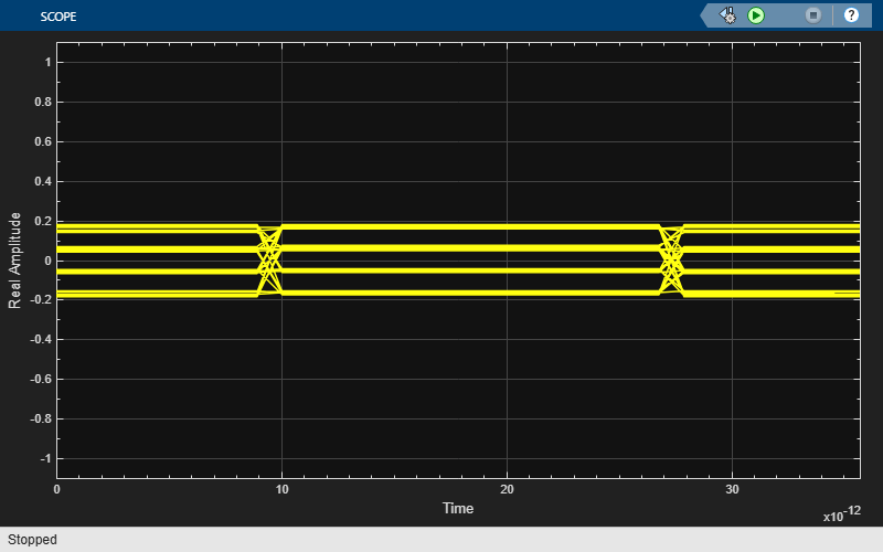
The simulation runs 40,000 PAM4 symbols at 56 GBaud (112 Gbps) with 16 samples per symbol (sample interval 1.12 ps). The electrical signal passes through the Tx, enters the optical domain at the ring modulator, propagates through fiber, and is converted back to electrical at the photodiode/TIA before reaching the Rx equalizer and eye diagram.
simOut = sim(model);
![Figure Init Statistical and Time Domain Analysis Results contains 4 axes objects and other objects of type uipanel. Axes object 1 with title Pulse Response, xlabel [s], ylabel [V] contains 2 objects of type line. These objects represent Unequalized, Equalized. Axes object 2 with title Waveform Derived from Pulse Response, xlabel [s], ylabel [V] contains 2 objects of type line. These objects represent Unequalized, Equalized. Axes object 3 with title Statistical Eye, xlabel [ps], ylabel [V] contains 10 objects of type image, line. Axes object 4 with title Time Domain Eye, xlabel [ps], ylabel [V] contains 10 objects of type image, line.](../../examples/serdes/ModelElectricalOpticalElectricalLinkExample_10.png)
Examining the Results
The simulation logs several signals for analysis. The eye diagram at the model output shows the received PAM4 signal after the complete electrical-optical-electrical path. We can also examine the ring transmission and temperature to understand the optical domain behavior.
logsout = simOut.logsout;
Ring Transmission
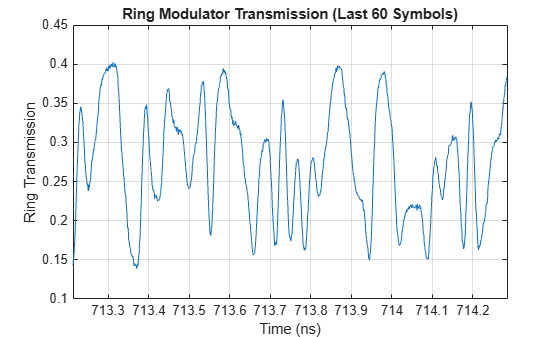
The ring transmission coefficient shows how the optical signal is modulated. Values near 1 mean the ring is nearly transparent (laser wavelength far from resonance); values near 0 mean most light is absorbed at resonance. The PAM4 modulation is visible in the waveform, with ISI from the bandwidth-limited optical path.
ringTr = logsout.getElement('Transmission').Values;
symbolTime = 1/56e9;  % 56 GBaud
tEnd = ringTr.Time(end);
tStart = tEnd - 60 * symbolTime;  % Show last 60 symbols

figure
plot(ringTr.Time * 1e9, squeeze(ringTr.Data))
xlim([tStart tEnd] * 1e9)
xlabel('Time (ns)')
ylabel('Ring Transmission')
title('Ring Modulator Transmission (Last 60 Symbols)')
grid on
Ring Temperature Rise
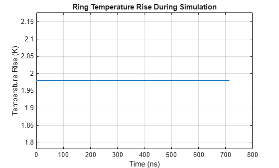
The ring temperature rise is initialized at the analytical steady state for the given initial absorbed power. The simulation window (~0.7 us) is much shorter than the dominant thermal time constant (~0.5 ms), so the temperature rise remains close to its initialized operating point. The narrow range of variation shows short-term thermal stability at this operating point. Longer simulations would be needed to observe full thermal settling, bi-stability, or drift.
tRing = logsout.getElement('RingTemp').Values;
figure
plot(tRing.Time * 1e9, squeeze(tRing.Data), 'LineWidth', 1.5)
xlabel('Time (ns)')
ylabel('Temperature Rise (K)')
title('Ring Temperature Rise During Simulation')
meanTemp = mean(squeeze(tRing.Data));
ylim([meanTemp * 0.9, meanTemp * 1.1])
grid on
Design Trade-Off: Laser-Ring Detuning
The detuning controls a three-way trade-off between modulation depth, linearity, and thermal stability. This is analogous to choosing the bias point of a nonlinear amplifier:
Small detuning (laser close to resonance): the PAM4 symbols sit on the steep slope of the Lorentzian and deep in the absorption notch resulting in large insertion loss and the ring absorbing more optical power, running hotter, and stronger thermal feedback. Modulation is also highly nonlinear (unequal level spacing).
Large detuning (laser far from resonance): the symbols sit on the flat top of the curve where the slope is shallow. The ring absorbs very little light, runs cool, and thermal behavior is stable. But voltage differences between PAM4 levels produce only small transmission changes, compressing the optical levels together and closing the eye (low OMA).
Optimal detuning: targets the steepest part of the slope (maximum change in transmission per volt), giving the best modulation efficiency at moderate absorption. As shown in the Thermo-Optic Feedback section, thermal self-heating shifts the effective detuning to ~0.10 nm at steady state, placing the laser about 0.3 FWHM from resonance; near the steepest slope.
This is the same trade-off as biasing a power amplifier near compression: more output swing but more self-heating and nonlinearity.
detunings = [0.03, 0.06, 0.10, 0.20];  % nm (0.10 is this model's optimal detuning)
vIn = linspace(-0.5, 0.5, 200);
pamVoltages = [-0.3, -0.1, 0.1, 0.3];
colors = lines(4);

figure
hold on
for idx = 1:length(detunings)
    d = detunings(idx);
    laserLam = ring.ResonanceWavelength - d;
    T = ring.getStaticTransmission(vIn, laserLam);
    if d == 0.10
        lw = 2.5;
    else
        lw = 1.2;
    end
    plot(vIn, T, 'LineWidth', lw, 'Color', colors(idx,:), ...
        'DisplayName', sprintf('\\Delta\\lambda = %.2f nm', d))
end
for v = pamVoltages
    xline(v, ':', 'Color', [0.5 0.5 0.5], 'HandleVisibility', 'off');
end
for idx = 1:length(detunings)
    d = detunings(idx);
    laserLam = ring.ResonanceWavelength - d;
    T_pam = ring.getStaticTransmission(pamVoltages, laserLam);
    hv = 'off';
    if idx == 1, hv = 'on'; end
    plot(pamVoltages, T_pam, 'o', 'Color', colors(idx,:), ...
        'MarkerSize', 7, 'MarkerFaceColor', colors(idx,:), ...
        'HandleVisibility', hv, 'DisplayName', 'PAM4 levels')
end
hold off
xlabel('Input Voltage (V)')
ylabel('Optical Transmission')
title('Ring Transfer Curve for Different Detunings')
legend('Location','best')
grid on
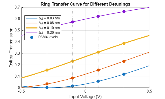
To read this plot: the filled dots mark where the four PAM4 drive voltages (-0.3, -0.1, 0.1, 0.3 V) land on each transfer curve. The optimal detuning ( = 0.10 nm, thick line) produces the widest vertical spread between levels with nearly equal spacing — the S-curve is centered on the voltage swing. At = 0.03 nm, all four levels are compressed near zero transmission (deep in the notch) with highly unequal spacing. At = 0.20 nm, all levels are compressed near the top of the curve where the slope is shallow — linear but with little contrast between them.
Design Trade-Off: Quality Factor
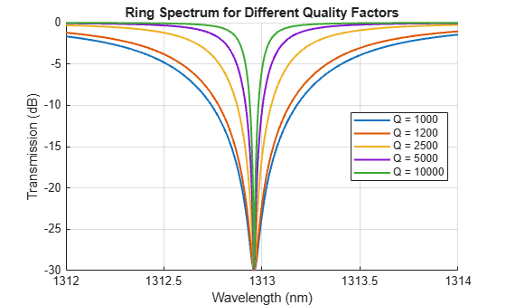
The quality factor Q controls the sharpness of the ring resonance. In SerDes terms, Q determines the "bandwidth" of the optical modulator:
Low Q (1000): broad notch with gentle slopes. Tolerant of wavelength drift and temperature changes, but the gentle slope means less modulation efficiency per volt; the transfer curve is flatter.
High Q (10000): narrow notch with steep slopes. Excellent modulation efficiency per volt, but extremely sensitive to temperature changes and requires precise wavelength control.
Most practical high-speed ring modulators use Q in the 2000-8000 range as a compromise. The model uses Q=4000, which balances modulation efficiency against photon-lifetime bandwidth as described in the Transfer Function section above. Higher Q designs offer steeper slopes (more modulation per volt) but further limit modulation bandwidth and increase thermal sensitivity.
Qs = [1000, 1200, 2500, 5000, 10000];
lam = linspace(1312.0, 1314.0, 2000);

figure
hold on
for q = Qs
    ring.Q = q;
    T = ring.getStaticTransmission(0, lam);
    plot(lam, 10*log10(T), 'LineWidth', 1.5, 'DisplayName', sprintf('Q = %d', q))
end
ring.Q = 4000;  % Restore model value
hold off
xlabel('Wavelength (nm)')
ylabel('Transmission (dB)')
title('Ring Spectrum for Different Quality Factors')
legend('Location','east')
grid on
Summary
This example demonstrated how to model a silicon photonic EOE redriver link using SerDes Toolbox with custom System objects for the optical domain. The key takeaways for SerDes engineers are:
Linear pluggable optics removes the retimer, requiring the host Rx to equalize through the entire E-O-E path. System-level IBIS-AMI simulation becomes essential for verifying link margin.
The ring modulator acts as a nonlinear VGA whose transfer curve depends on the laser-ring wavelength offset (detuning) and temperature. The quality factor Q controls the linearity vs. modulation depth trade-off.
Thermo-optic feedback causes data-dependent drift of the operating point, similar to self-heating effects in high-power drivers.
The AGC + VGA pair normalizes the signal: the AGC sets the optimal ring drive amplitude on input, and the VGA sets the output swing for the downstream channel; analogous to input/output stages of an electrical redriver.
The AC coupling stage bridges the unipolar optical domain back to the differential signaling convention of IBIS-AMI.
The SerDes Toolbox framework (AMI models, CTLE, DFE, eye diagrams) works end-to-end; the optical components simply replace a section of the electrical channel, and standard datapath blocks (CTLE, AGC, VGA, Pass-Through with custom System objects) provide the electrical conditioning.

