Designing Multi-Stage RF Front-End: From Individual Components to Unified PCB Layout
R2026bThis example shows how to design a three-stage 2.4 GHz RF receiver front end using RF PCB Toolbox. Then compare two RF system-level analysis approaches: circuit-level composition and full-wave electromagnetic simulation..
System requirement: A wireless receiver operating at 2.4 GHz requires a preselector filter to reject out-of-band interference, an inline power monitor to track received signal strength without breaking the signal chain, and an impedance matching network to interface the 50 Ohm system with a downstream low-noise amplifier (LNA) whose input impedance is 75 Ohm.
The front end consists of three cascaded stages:
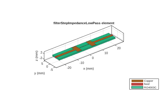
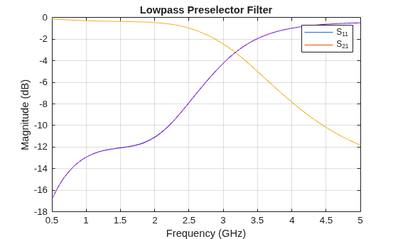
Stepped-impedance lowpass filter (LPF) — The filter rejects signals above 3 GHz while passing the 2.4 GHz band with low insertion loss.
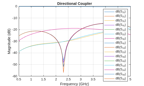
Directional coupler — The coupler taps ~1% of the through power (~20 dB coupling) to a monitoring port. A power detector on the coupled port measures signal strength in real time. The main-path signal passes through with minimal loss (~0.2 dB).
Quarter-wave matching network — The matching network transforms the 50 Ohm system impedance to the 75 Ohm LNA input impedance using a microstrip line whose characteristic impedance  .
.
S-parameter results are re-normalized to the mixed reference impedance (50 Ohm at the input, 75 Ohm at the output). The matching network is evaluated against its designed load, and the return loss at the output reflects true system performance.
Analysis approaches compared:
Circuit-level composition — Each stage is converted to a pcbElement and wired into an RF Toolbox circuit object for fast cascaded S-parameter analysis. This approach is quick but assumes ideal isolation between stages.
Full-wave pcbComponent assembly — The conductor geometry from each stage is extracted, positioned on a single board, and combined into a unified pcbComponent. Method of Moments (MoM) simulation captures inter-stage EM coupling, fringing fields, and parasitic effects.
Requires: RF PCB Toolbox, RF Toolbox
Design Specifications
Define the operating frequency, filter cutoff, impedance levels, and substrate parameters. Rogers RO4003C is a common low-loss substrate for microwave circuits.
f0   = 2.4e9;             % Operating frequency [Hz]
fmax = 3e9;               % Lowpass filter cutoff [Hz]
Z0   = 50;                % System impedance [Ohm]
ZL   = 75;                % LNA input impedance [Ohm]

er   = 3.55;              % Relative permittivity
h    = 0.813e-3;          % Substrate thickness [m]
tanD = 0.0027;            % Loss tangent
sub  = dielectric(EpsilonR=er, LossTangent=tanD, Name="RO4003C", Thickness=h);
cond = metal("Copper");

freq = linspace(0.5e9, 5e9, 101);

designSpecs = table( ...
    [f0/1e9; fmax/1e9; Z0; ZL; er; h*1e3], ...
    ["Operating frequency"; "LPF cutoff"; "System impedance"; ...
     "LNA impedance"; "Permittivity"; "Substrate thickness"], ...
    ["GHz"; "GHz"; "Ohm"; "Ohm"; ""; "mm"], ...
    VariableNames=["Value", "Parameter", "Unit"]);
designSpecs = designSpecs(:, ["Parameter", "Value", "Unit"]);
designSpecs
designSpecs = 6×3 table
          Parameter          Value    Unit
    _____________________    _____    _____

    "Operating frequency"      2.4    "GHz"
    "LPF cutoff"                 3    "GHz"
    "System impedance"          50    "Ohm"
    "LNA impedance"             75    "Ohm"
    "Permittivity"            3.55    ""
    "Substrate thickness"    0.813    "mm"
Stage 1: Stepped-Impedance Lowpass Preselector Filter
The preselector filter is the first element in the receive chain. It passes signals in the 2.4 GHz band and rejects out-of-band interference above 3 GHz. A stepped-impedance topology alternates between high- and low-impedance microstrip sections to realize the lowpass response.
Set substrate, height, and conductor properties before calling design so the geometry is sized correctly for the RO4003C substrate.
lpf = filterStepImpedanceLowPass;
lpf.Substrate = sub;
lpf.Height    = h;
lpf.Conductor = cond;
lpf = design(lpf, fmax);

figure
show(lpf)
Compute S-parameters using the Method of Moments (MoM) solver.
sparLPF = sparameters(lpf, freq);
figure
rfplot(sparLPF)
title('Lowpass Preselector Filter')
legend('S_{11}', 'S_{21}')
grid on
Stage 2: Directional Coupler for Inline Power Monitoring
The directional coupler sits between the preselector and the matching network. It samples a small fraction of the through power (~1%, or approximately 20 dB coupling) and routes it to a monitoring port where a power detector (e.g., diode or ADC) can measure received signal strength in real time. The through port carries the main signal with minimal insertion loss.
The couplerDirectional catalog object does not support design function, so coupler geometry is specified directly: Set its length to a quarter guided-wavelength at the operating frequency.
c0 = 3e8;
er_eff = (er + 1)/2 + ((er - 1)/2) * (1 + 12*h/1.84e-3)^(-0.5);
lambda_g = c0 / (f0 * sqrt(er_eff));
coupledLength = lambda_g / 4;

dc = couplerDirectional;
dc.Length            = coupledLength;
dc.Width             = 1.84e-3;
dc.Spacing           = 0.5e-3;
dc.Height            = h;
dc.PortLineWidth     = 1.84e-3;
dc.GroundPlaneLength = coupledLength + 30e-3;
dc.GroundPlaneWidth  = 20e-3;
dc.Substrate         = sub;
dc.Conductor         = cond;

figure
show(dc)
title('Stage 2: Directional Coupler')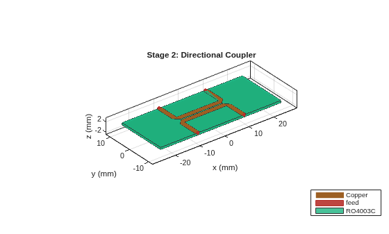
Compute full-wave S-parameters. The coupler is a 4-port device:
Port 1 is the signal input port.
Port 2 is the signal through-port (signal path continues from here).
Port 3 is a coupled port for monitoring power output.
Port 4 is isolated (terminated in 50 Ohm in practice).
sparDC = sparameters(dc, freq);

figure
rfplot(sparDC)
title('Directional Coupler')
grid on
Evaluate coupler performance at the operating frequency.
couplerPerf = table( ...
    [coupling(dc, f0); directivity(dc, f0); isolation(dc, f0)], ...
    ["Coupling"; "Directivity"; "Isolation"], ...
    VariableNames=["dB", "Metric"]);
couplerPerf = couplerPerf(:, ["Metric", "dB"]);
couplerPerf
couplerPerf = 3×2 table
       Metric          dB
    _____________    ______

    "Coupling"       -18.38
    "Directivity"    -16.75
    "Isolation"      -35.13
Stage 3: Quarter-Wave Matching Network (50 Ohm to 75 Ohm)
The matching network is the final stage before the LNA. Often LNA devices present an input impedance different from the standard system impedance of 50 Ohm. In this example, the LNA input is 75 Ohm. A quarter-wave microstrip transformer provides a narrowband impedance match at the operating frequency.
The transformer characteristic impedance is the geometric mean of the source (Z0) and load (ZL) impedance:

For this impedance calculate the microstrip width using standard synthesis formulas, with line length of one quarter guided-wavelength at 2.4 GHz.
ZT = sqrt(Z0 * ZL);
matchDesign = table(ZT, "Ohm", ...
    VariableNames=["Transformer Impedance", "Unit"]);
matchDesign
matchDesign = 1×2 table
    Transformer Impedance    Unit
    _____________________    _____

           61.237            "Ohm"
A_val = (ZT/60)*sqrt((er+1)/2) + ((er-1)/(er+1))*(0.23 + 0.11/er);
Wh = 8*exp(A_val) / (exp(2*A_val) - 2);
if Wh > 2
    B_val = 377*pi / (2*ZT*sqrt(er));
    Wh = (2/pi)*(B_val - 1 - log(2*B_val - 1) + ...
        ((er-1)/(2*er))*(log(B_val-1) + 0.39 - 0.61/er));
end
wMatch = Wh * h;

matchLine = microstripLine;
matchLine.Length          = lambda_g / 4;
matchLine.Width           = wMatch;
matchLine.Height          = h;
matchLine.GroundPlaneWidth = 18e-3;
matchLine.Substrate       = sub;
matchLine.Conductor       = cond;

figure
show(matchLine)
title(sprintf('Stage 3: Quarter-Wave Transformer (Z_T = %.1f \\Omega)', ZT))
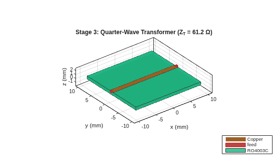
Compute the S-parameters of the matching network.
sparMatch = sparameters(matchLine, freq);

figure
rfplot(sparMatch)
title('Quarter-Wave Matching Network')
legend('S_{11}', 'S_{21}')
grid on
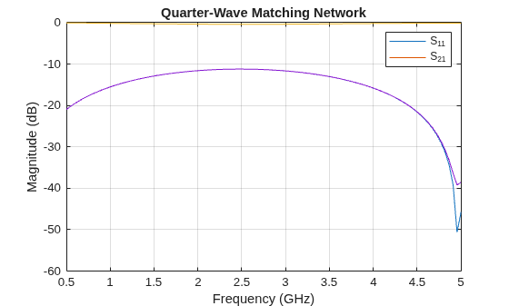
Approach 1: Circuit-Level Composition
Convert the filter, coupler, and matching line objects into a pcbElement and wire them into an RF Toolbox circuit object. This enables the use of fast cascaded S-parameter analysis that ignores inter-stage EM coupling.
For the couplerDirectional, a full-wave solution is used automatically since behavioral pcbElement is not supported.
Route the main signal path through the LPF, the coupler's through port, and the matching network.Terminate the coupled and isolated ports in 50 Ohm loads.
warning off;
elemMatch = pcbElement(matchLine);
elemLPF = pcbElement(lpf);
elemDC = pcbElement(dc);
ckt = circuit;
add(ckt, [1 2 0 0], elemLPF);
add(ckt, [2 3 5 6 0 0 0 0], elemDC);
add(ckt, [6 0], resistor(Z0));
add(ckt, [5 0], resistor(Z0));
add(ckt, [3 4 0 0], elemMatch);
setports(ckt, [1 0], [4 0]);
Compute cascaded S-parameters. Because the output terminates in 75 Ohm (the LNA), use newref to re-normalize the S-parameters to mixed reference impedance. The circuit/sparameters function only accepts a scalar reference impedance. First compute at 50 Ohm and then re-normalize to [50 75] Ohm.
Zref_ckt = [Z0 ZL];
sparChain50 = sparameters(ckt, freq, Z0);
sparChain   = newref(sparChain50, Zref_ckt);

figure
rfplot(sparChain)
title('Circuit-Level Front-End (Zref = [50 75] \Omega)')
legend('S_{11} (Input Match)', 'S_{21} (Insertion)')
grid on
![Figure contains an axes object. The axes object with title Circuit-Level Front-End (Zref = [ 50 75 ] Omega ), xlabel Frequency (GHz), ylabel Magnitude (dB) contains 4 objects of type line. These objects represent S_{11} (Input Match), S_{21} (Insertion), dB(S_{12}), dB(S_{22}).](../../examples/rfpcb/DesigningMultiStageRFFrontEndExample_09.png)
Compare the cascaded circuit response with individual stage responses.
figure
tiledlayout(2, 1)

nexttile
hold on
plot(freq/1e9, 20*log10(abs(squeeze(sparLPF.Parameters(1,1,:)))), ...
    '--', 'LineWidth', 1.5, 'DisplayName', 'LPF only')
plot(freq/1e9, 20*log10(abs(squeeze(sparChain.Parameters(1,1,:)))), ...
    '-', 'LineWidth', 2, 'DisplayName', 'Full chain')
ylabel('|S_{11}| (dB)')
xlabel('Frequency (GHz)')
title('Return Loss')
legend('Location', 'best')
grid on
hold off

nexttile
hold on
plot(freq/1e9, 20*log10(abs(squeeze(sparLPF.Parameters(2,1,:)))), ...
    '--', 'LineWidth', 1.5, 'DisplayName', 'LPF only')
plot(freq/1e9, 20*log10(abs(squeeze(sparMatch.Parameters(2,1,:)))), ...
    '-.', 'LineWidth', 1.5, 'DisplayName', 'Match only')
plot(freq/1e9, 20*log10(abs(squeeze(sparChain.Parameters(2,1,:)))), ...
    '-', 'LineWidth', 2, 'DisplayName', 'Full chain')
ylabel('|S_{21}| (dB)')
xlabel('Frequency (GHz)')
title('Insertion Loss')
legend('Location', 'best')
grid on
hold off

sgtitle('Individual Stages vs. Complete Front-End (Circuit)')
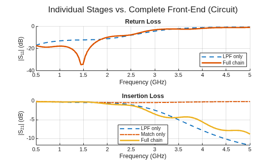
Approach 2: Full-Wave Simulation on a Unified PCB Layout
The circuit-level approach treats each stage as an isolated block. In a real PCB, the stages are physically close together and share a common substrate and ground plane. Fringing fields, surface currents, and inter-stage coupling can shift the frequency response and degrade return loss.
To capture these effects, the conductor geometry from each catalog object is extracted, translated into position on a single board, and combined into a unified pcbComponent. The MoM solver then simulates the entire structure as one electromagnetic problem.
Step 1 — Extract geometry Wrapping each catalog object in pcbComponent exposes its conductor shapes (Layers{1}) and feed locations. Because shape objects are handle classes, use copy before translate to avoid mutating the originals.
lpfPCB   = pcbComponent(lpf);
dcPCB    = pcbComponent(dc);
matchPCB = pcbComponent(matchLine);
Step 2 — Compute translation offsets The LPF stays at the origin. Shift the directional coupler so its bottom input port (port 1) aligns with the LPF output port (port 2). Shift the matching network so its input port aligns with the coupler through port (port 2). Apply an additional 1 mm overlap extension at each junction so the conductor traces physically overlap, ensuring a robust galvanic connection between stages
lpfFeed2   = lpfPCB.FeedLocations(2, 1:2);
dcFeed1    = dcPCB.FeedLocations(1, 1:2);
dcFeed2    = dcPCB.FeedLocations(2, 1:2);
matchFeed1 = matchPCB.FeedLocations(1, 1:2);

overlapExt   = 1e-3;
dc_offset    = lpfFeed2 - dcFeed1 - [overlapExt 0];
match_offset = (dcFeed2 + dc_offset) - matchFeed1 - [overlapExt 0];

offsetTable = table( ...
    ["DC"; "Match"], ...
    [dc_offset(1)*1e3; match_offset(1)*1e3], ...
    [dc_offset(2)*1e3; match_offset(2)*1e3], ...
    [overlapExt*1e3; overlapExt*1e3], ...
    VariableNames=["Stage", "X_mm", "Y_mm", "Overlap_mm"]);
offsetTable
offsetTable = 2×4 table
     Stage      X_mm     Y_mm    Overlap_mm
    _______    ______    ____    __________

    "DC"       30.714     10         1
    "Match"    48.447      0         1
Step 3 — Translate and combine conductor shapes Copy and translate the top conductor layers to their computed positions, and merge using Boolean union. Form the inter-stage connections by the physical overlap of the port-line traces — separate connecting traces or feed pins are not needed at the junctions.
lpfTopCopy   = copy(lpfPCB.Layers{1});
dcTopCopy    = copy(dcPCB.Layers{1});
matchTopCopy = copy(matchPCB.Layers{1});

dcTopCopy = translate(dcTopCopy,    [dc_offset    0]);
matchTopCopy = translate(matchTopCopy, [match_offset 0]);

combinedTop = lpfTopCopy + dcTopCopy + matchTopCopy;
Step 4 — Build the board and ground plane Size the rectangular board to the exact bounding box of the conductor traces so that feed pins sit at the board edges with no extra margin. To compute the bounds, collect Polygon vertices (for the LPF and coupler) and rectangle corners (for the matching line)..
lpfV = lpfTopCopy.Vertices;
lpfV = lpfV(~isnan(lpfV(:,1)), 1:2);
dcV  = dcTopCopy.Vertices;
dcV  = dcV(~isnan(dcV(:,1)), 1:2);
mCx  = matchTopCopy.Center(1);
mCy  = matchTopCopy.Center(2);
matchCorners = [mCx - matchTopCopy.Length/2, mCy - matchTopCopy.Width/2;
    mCx + matchTopCopy.Length/2, mCy + matchTopCopy.Width/2];

allX = [lpfV(:,1); dcV(:,1); matchCorners(:,1)];
allY = [lpfV(:,2); dcV(:,2); matchCorners(:,2)];

xMin = min(allX);
xMax = max(allX);
yMin = min(allY);
yMax = max(allY);

boardLength  = xMax - xMin;
boardWidth   = yMax - yMin;
boardCenterX = (xMax + xMin) / 2;
boardCenterY = (yMax + yMin) / 2;

boardShape  = antenna.Rectangle(Length=boardLength, Width=boardWidth, ...
    Center=[boardCenterX boardCenterY]);
groundPlane = traceRectangular(Length=boardLength, Width=boardWidth, ...
    Center=[boardCenterX boardCenterY]);

boardSize = table(boardLength*1e3, boardWidth*1e3, ...
    VariableNames=["Length_mm", "Width_mm"]);
boardSize
boardSize = 1×2 table
Length_mm Width_mm
_________ ________
80.161 23.167
Step 5 — Define external feed locations Only the four external ports need feed pins. Internal connections between stages are handled by conductor overlap.
Port 1: LPF input (system input, 50 Ohm)
Port 2: Coupler coupled port (power monitor)
Port 3: Coupler isolated port (terminated)
Port 4: Match output (LNA interface, 75 Ohm
feed1 = [lpfPCB.FeedLocations(1, 1:2),                    1, 3];
feed2 = [dcPCB.FeedLocations(3, 1:2)  + dc_offset,        1, 3];
feed3 = [dcPCB.FeedLocations(4, 1:2)  + dc_offset,        1, 3];
feed4 = [matchPCB.FeedLocations(2, 1:2) + match_offset,   1, 3];

portLocations = table( ...
    ["Port 1 (In)"; "Port 2 (Coupled)"; "Port 3 (Isolated)"; "Port 4 (Out)"], ...
    [feed1(1)*1e3; feed2(1)*1e3; feed3(1)*1e3; feed4(1)*1e3], ...
    [feed1(2)*1e3; feed2(2)*1e3; feed3(2)*1e3; feed4(2)*1e3], ...
    VariableNames=["Port", "X_mm", "Y_mm"]);
portLocations
portLocations = 4×3 table
           Port             X_mm      Y_mm
    ___________________    _______    ____

    "Port 1 (In)"          -22.348      0
    "Port 2 (Coupled)"      21.348     20
    "Port 3 (Isolated)"      40.08     20
    "Port 4 (Out)"          57.813      0
Step 6 — Assemble the pcbComponent and set mesh parameters Apply a coarser mesh (MaxEdgeLength ~ lambda_g/8, GrowthRate = 0.7) to reduce the number of mesh triangles and speed up the MoM solver.
pcbManual = pcbComponent;
pcbManual.BoardShape     = boardShape;
pcbManual.BoardThickness = h;
pcbManual.Layers         = {combinedTop, sub, groundPlane};
pcbManual.FeedLocations  = [feed1; feed2; feed3; feed4];
pcbManual.FeedDiameter   = min([lpfPCB.FeedDiameter, ...
    dcPCB.FeedDiameter, matchPCB.FeedDiameter]);


figure
show(pcbManual)
title('Combined RF Front-End — Unified PCB Layout')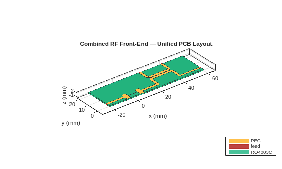
Step 7 — Full-wave simulation Compute S-parameters for the 4-port structure using the MoM solver with adaptive interpolation, then re-normalize port 4 to 75 Ohm using newref.
sparManual50 = sparameters(pcbManual, freq);

Zref_pcb   = [Z0 Z0 Z0 ZL];
sparManual = newref(sparManual50, Zref_pcb);

figure
rfplot(sparManual)
title('Full-Wave S-Parameters (Zref = [50 50 50 75] \Omega)')
grid on
![Figure contains an axes object. The axes object with title Full-Wave S-Parameters (Zref = [ 50 50 50 75 ] Omega ), xlabel Frequency (GHz), ylabel Magnitude (dB) contains 16 objects of type line. These objects represent dB(S_{11}), dB(S_{21}), dB(S_{31}), dB(S_{41}), dB(S_{12}), dB(S_{22}), dB(S_{32}), dB(S_{42}), dB(S_{13}), dB(S_{23}), dB(S_{33}), dB(S_{43}), dB(S_{14}), dB(S_{24}), dB(S_{34}), dB(S_{44}).](../../examples/rfpcb/DesigningMultiStageRFFrontEndExample_12.png)
Display 4-port results at the operating frequency. The main signal path is Port 1 to Port 4, so the through response is S41.
[~, idxF0] = min(abs(freq - f0));
S11_manual = 20*log10(abs(squeeze(sparManual.Parameters(1,1,:))));
S41_manual = 20*log10(abs(squeeze(sparManual.Parameters(4,1,:))));

fullWaveResults = table( ...
    ["S11 (return)"; "S41 (through)"; "S21 (coupled)"; "S31 (isolated)"], ...
    [S11_manual(idxF0); S41_manual(idxF0); ...
     20*log10(abs(sparManual.Parameters(2,1,idxF0))); ...
     20*log10(abs(sparManual.Parameters(3,1,idxF0)))], ...
    VariableNames=["Parameter", "dB"]);
fullWaveResults
fullWaveResults = 4×2 table
       Parameter          dB
    ________________    _______

    "S11 (return)"      -6.4143
    "S41 (through)"     -1.2999
    "S21 (coupled)"     -20.215
    "S31 (isolated)"    -27.852
Comparison: Circuit vs. Full-Wave
The circuit model assumes each stage is electromagnetically isolated, while the full-wave model simulates the complete PCB as one structure. Differences in S-parameters approaches reveal the impact of inter-stage coupling, substrate surface waves, and shared-ground-plane currents.
S11_circuit = 20*log10(abs(squeeze(sparChain.Parameters(1,1,:))));
S21_circuit = 20*log10(abs(squeeze(sparChain.Parameters(2,1,:))));

figure
tiledlayout(2, 1)

nexttile
hold on
plot(freq/1e9, S11_circuit, '--', 'LineWidth', 1.5, ...
    'DisplayName', 'Circuit S_{11}')
plot(freq/1e9, S11_manual, '-', 'LineWidth', 2, ...
    'DisplayName', 'Full-Wave S_{11}')
ylabel('|S_{11}| (dB)')
xlabel('Frequency (GHz)')
title('Return Loss')
legend('Location', 'best')
grid on
hold off

nexttile
hold on
plot(freq/1e9, S21_circuit, '--', 'LineWidth', 1.5, ...
    'DisplayName', 'Circuit S_{21}')
plot(freq/1e9, S41_manual, '-', 'LineWidth', 2, ...
    'DisplayName', 'Full-Wave S_{41}')
ylabel('|S_{through}| (dB)')
xlabel('Frequency (GHz)')
title('Insertion Loss')
legend('Location', 'best')
grid on
hold off

sgtitle('Circuit Composition vs. Full-Wave PCB Simulation')
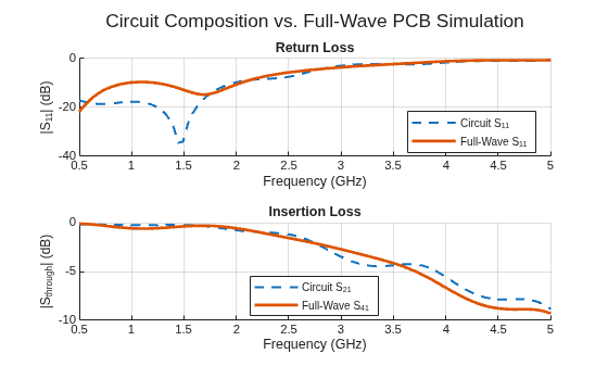
Summary
This example demonstrated two approaches to multi-stage RF front-end analysis:
Designed three PCB components on Rogers RO4003C substrate: a stepped-impedance lowpass filter, a directional coupler for power monitoring, and a quarter-wave matching network for a 75 Ohm LNA.
In circuit-level comparison converted each component to a
pcbElement, wired them into an RF Toolboxcircuit, and computed S-parameters with mixed reference impedance ([50 75] Ohm) usingnewref.In full-wave
pcbComponentassembly extracted conductor geometry from each catalog object usingpcbComponentwrappers, positioned the shapes on a single board usingcopyandtranslate, built a unifiedpcbComponentwith tight board edges and coarse mesh control, and ran a MoM simulation re-normalized to [50 50 50 75] Ohm.Compared the results to quantify how inter-stage EM coupling affects return loss and insertion loss in the physical layout.

