PCB Viewer
Description
The PCB Viewer app allows you to import, visualize, inspect, and navigate printed circuits boards (PCBs).
Using this app you can:
Import one or more PCB database files: ODB++ and native formats.
View the PCB layout, and navigate around the layout using the zoom and pan features. You can select which PCB layers and elements to display.
Set user preferences including board opacity, grid visibility, and measurement units.
Point-and-click on the board layout display to select PCB objects: components, pins, vias, segments, nets, and areas. You can choose which types of objects are selectable.
Inspect lists of PCB database elements including parts, nets, components, and padstacks.
Search for specific elements in the PCB database.
Inspect the properties of individual PCB objects by either clicking on the object in the layout, or by selecting the object in the database lists.
Measure the physical distance between elements in the PCB layout.
Add annotated notes to the PCB layout.
Save and open PCB Viewer sessions.
Export PCB layouts.
Open the PCB Viewer App
MATLAB® Toolstrip: On the Apps tab, under RF and Mixed Signal, click the PCB Viewer app icon.
MATLAB command prompt: Enter
pcbViewer.
Examples
To open the app, type this code in the Command Window. Alternatively, in the MATLAB Toolstrip click on the PCB Viewer icon in the Apps tab under RF and Mixed signal.
pcbViewer
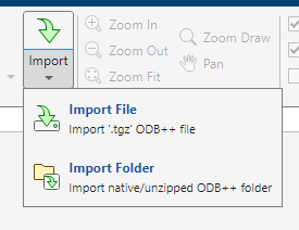
Click Import and then Import File or **Import Folde**r to import a PCB database file or folder.

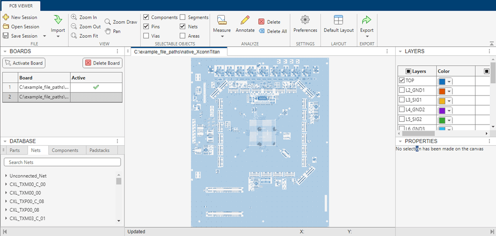
Select a PCB database file or folder from the path where the file or folder is located. After the importing is completed the layout of the board is visible in the canvas pane.
Additional panes become visible in the app window.
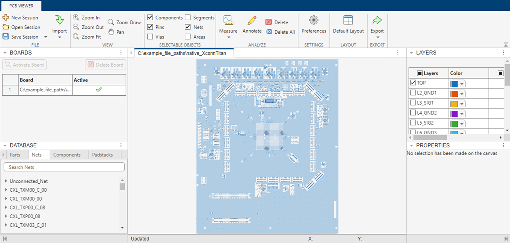
Note that in the BOARDS pane above the current (and only) board is Active, as indicated by the check mark.
Additional PCB databases can be imported into the current session resulting in a list of boards in the BOARDS pane.
The active board may be changed by selecting from the list of boards, and clicking Activate Board. Boards in the list may also be deleted.

Once you have imported all the PCB databases you need, you can save the session as a '.mat' file. Click on Save Session. Saving a session saves time when restarting the App, since all the imported boards will be automatically reloaded when a session is opened.
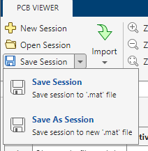
The session name is located the upper left area above the App name..
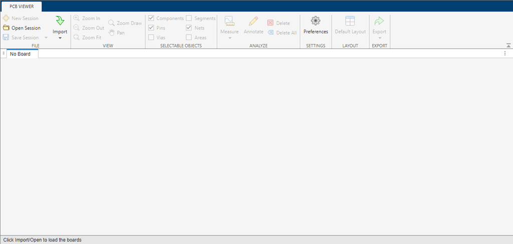
Open the App.
pcbViewer
Once the App is running you can import a PCB, or open a previously saved session by clicking Open Session in the tool bar. Select the desired '.mat' file.
![]()
The PCB database files saved in the session will automatically open.
Visualize the PCB
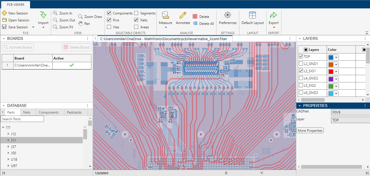
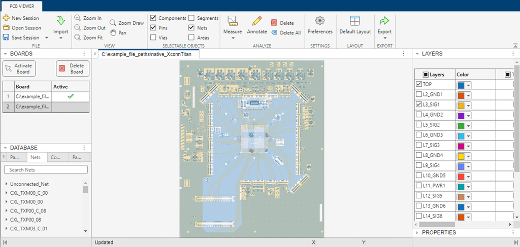
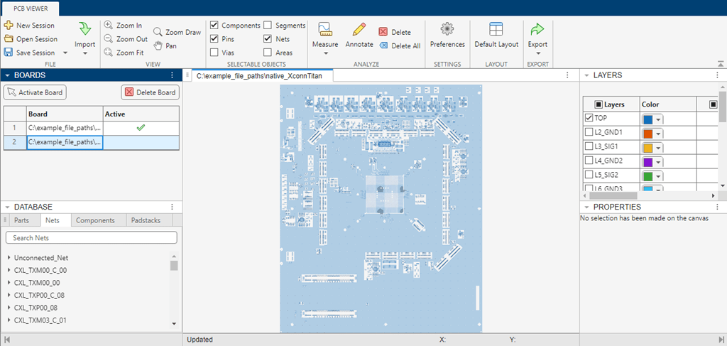
You can visualize one or more board layers using the LAYERS pane. Expand the pane by clicking the three dots in pane top bar. Expanding the pane will make it easier to use.
Use the check boxes in the Layers column to select one or more Layers to be visible in the canvas pane, and use the check boxes in the corresponding elements columns (Trace, Pins, Via, Area) to select which PCB elements are visible in a layer.
Here two layers, and all elements in each layer, are selected.
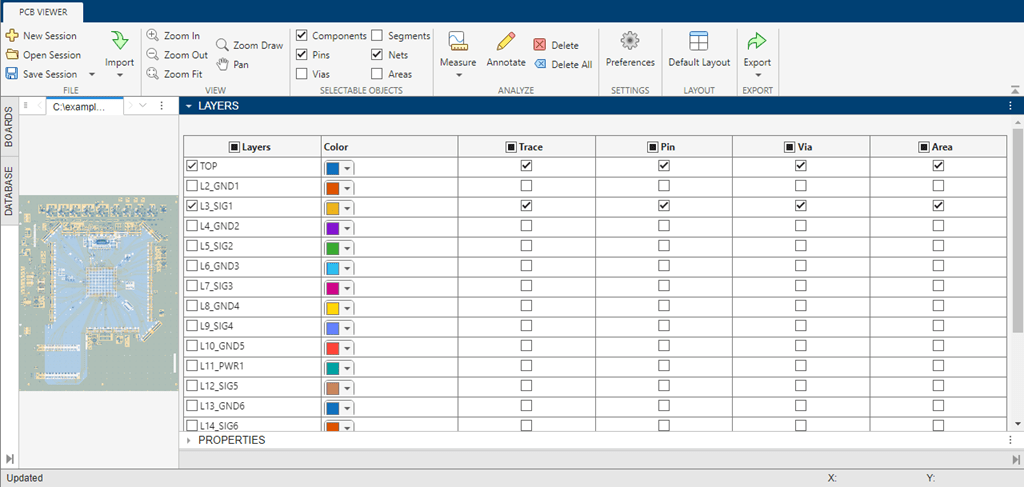
Click on Default Layout in the toolbar to restore the pane to it's original size.
In the DATABASE pane click on one of the tabs to select a PCB element. For this example click Nets. The list of the board's nets appears.
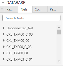
You can search for an element by typing its name in the the Search box.
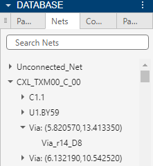
Click on the right arrow of a net and a list of connections associated with the Net will appear.
Additional details may be inspected by clicking on the right arrow of individual connections.
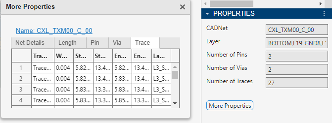
Click an individual element name to display its properties in the Properties pane.
The PROPERTIES pane also gets populated when you select a PCB element in the canvas pane.
Clicking More Properties creates a separate pop-up window showing additional component properties.
Measure and annotate PCBs with PCB Viewer App
Launch the PCB Viewer App and then import a PCB database file, or open a previously saved PCB Viewer session.
pcbViewer
Click on Import in the tool bar to import one or more PCB database files or folders.
Alternatively, click on Open Session in the tool bar to open a previously saved PCB Viewer session ('.mat' file). The session PCB databases will automatically be loaded.
![]()
Select a PCB in the Boards pane for measurements. Make sure that the selected board is active as indicated by the green check mark.
Click Measure in the toolbar.
In this example select point-to-point measurement to measure the distance between two points in the layout.
You can also click Measure to set:
Snap Options: where the end points are located in an element.
Direction: choose along which axes the measurement occurs.
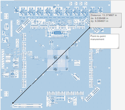
Use the cross-hair marker to select the measurement points on the layout. A line appears between the measurements points, and a box shows the measurement results.
You can make multiple measurements in a layout.
Click Annotate to add an annotated note in the layout. Type the annotation in the box.
Click Delete or Delete All to delete measurements and annotations.
Parameters
Version History
Introduced in R2026a